Magneto-Electric Voltage Controlled Spin Transistors

a technology of magnetic voltage control and spin transistor, which is applied in the field of magnetic voltage control of spin transistor, can solve the problem of extremely limited spatial densities of arrays of such more conventional spin transistors

Active Publication Date: 2014-08-21
QUANTUM DEVICES +1
View PDF2 Cites 26 Cited by
  • Summary
  • Abstract
  • Description
  • Claims
  • Application Information

AI Technical Summary

Benefits of technology

[0013]Quantum mechanical exchange coupling between the boundary magnetization and the spins of the carriers in the narrow channel of the FET gives rise to damped precession of the spins injected from the source of the FET into the channel. When utilizing channel materials with virtually zero spin-orbit coupling, such as graphene or Si, the effective exchange field of the voltage-controlled boundary magnetization is the sole source for spin precession. If the narrow channel conductor is sufficiently thin, the transport channel will be spin polarized by the proximity effect, providing coherent spin transport or modulated spin precession. For a given remanent boundary magnetization, the exchange field will determine the spin state of the carriers at the analyzer (FM drain) in concert with the length of the channel. Electrical spin injection and controlled spin precessional motion in silicon lateral transport devices using externally applied magnetic fields at room temperature and above has been demonstrated [van't Erve 07, Jonker 07]. Spin field effect transistors [Dery 07, Semenov 07, Semenov 10, Zaliznyak 10], have certainly been described using graphene and other narrow channel conductors.

Problems solved by technology

Addition wiring to create fringe fields is needed, and the spatial densities of an array of such more conventional spin-FET is extremely limited because the extrinsic magnetic fields will be difficult to restrict, without the stray fields influencing adjacent transistors in any dense array.

Method used


Image

  • Magneto-Electric Voltage Controlled Spin Transistors
  • Magneto-Electric Voltage Controlled Spin Transistors
  • Magneto-Electric Voltage Controlled Spin Transistors

Examples


Embodiment Construction

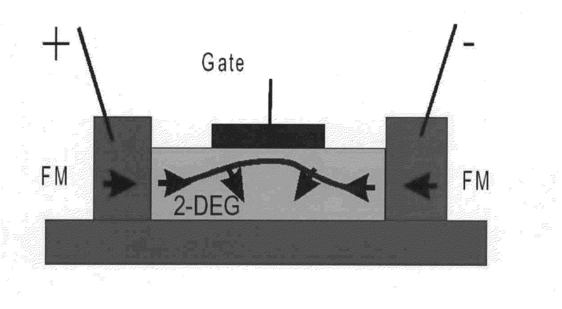
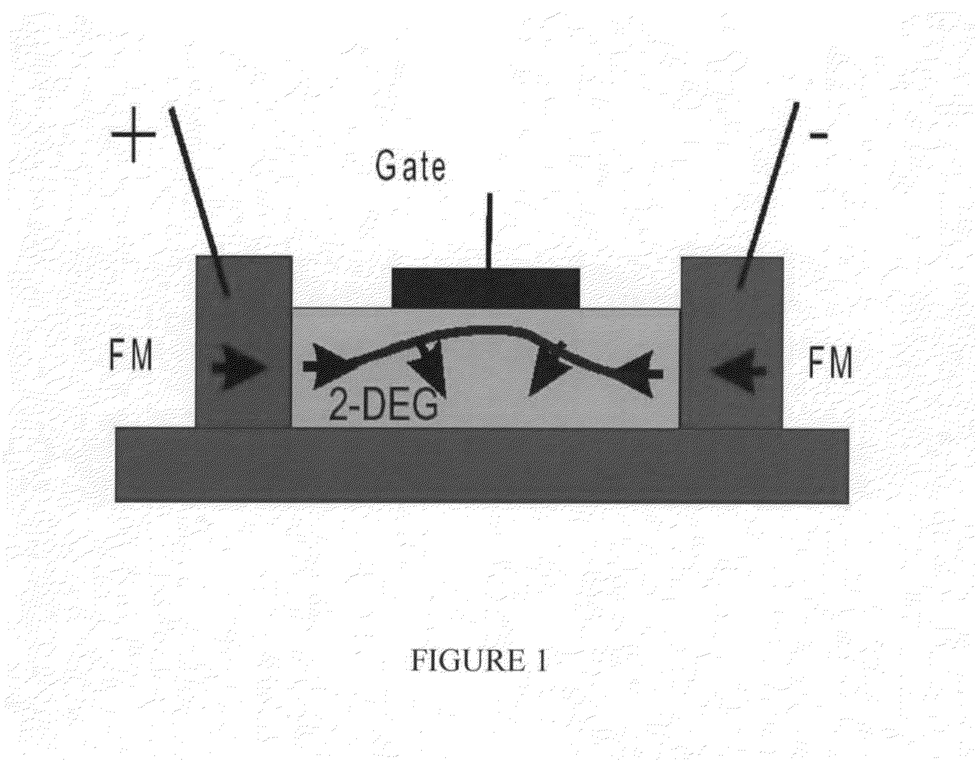
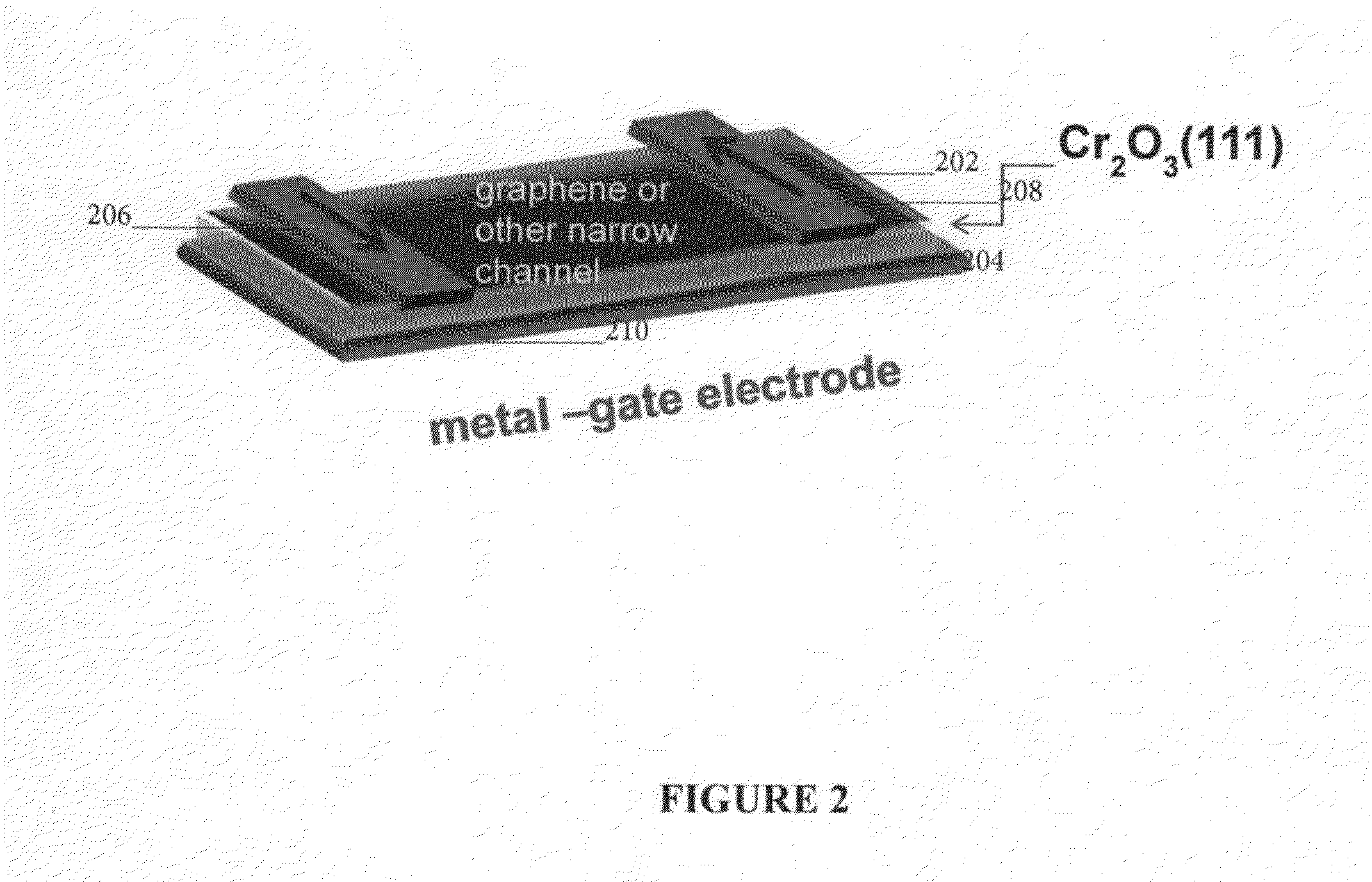
[0021]The device described below works because of the huge interface polarization of dielectric chromia (described below as the gate dielectric). This boundary polarization is voltage controlled and described above [He 10, Belashchenko 10, Wang 14]. The narrow channel (i.e. thin) conductor (graphene, InP, GaSb, PbS, MoS2, WS2, MoSe2, WSe2, etc.) of the FET schemes described below are polarized by this very high interface polarization, a proximity effect. The proximity effect was originally described as a mean field effect in magnetism, not directly attributed to any specific material and is embodied by the Landau-Ginzburg equation, for which solutions are known for some boundary conditions [Dowben 91, Miller 93]. We need to divide the concept into actually two types of devices nonetheless.

[0022](A) The Large Field, Very Short Channel Regime:

[0023]Conduction bands are strongly exchange-split. Spin precession length is microscopic, and spins completely decohere over small lengths, or ...


PUM


Abstract

The invention relates to a magneto-electric spin-FET including a gate film of chromia and a thin film of a conductive channel material which may be graphene, InP, GaAs, GaSb, PbS, MoS2, WS2, MoSe2, WSe2 and mixtures thereof. The chromia, or other magneto-electric, and conduction channel material are in intimate contact along an interface there between. The resulting magneto-electric device may be voltage-controlled and provide non-volatile memory.

Description

BACKGROUND OF THE INVENTION[0001]This patent application is related to pending U.S. patent application Ser. No. 13 / 343,970 filed Jan. 5, 2012, entitled COHERENT SPIN FIELD EFFECT TRANSISTOR. This application is also related to U.S. Patent Application 61 / 936,399 entitled Voltage Switchable Non-Local Spin-FET and Methods of Making Same. The disclosures of both these application are incorporated-by-reference herein.[0002]This application claims benefit of the filing date of Provisional Patent Application 61 / 766,025 filed Feb. 18, 2013. The entire disclosure of the benefit application is incorporated herein-by-reference.[0003]Aspects of the inventions disclosed and claimed herein were made in the course of work supported by funding grant NSF / MRSEC DMR-0820521. The United States Government may have certain rights in and to those inventions. The inventions disclosed and claimed herein were also made with the support of SRC Funding, including SRC-NRI Task I.D. 2101.01, GRC Nanomanufacturin...

Claims


Application Information

Patent Timeline
Patent Type & Authority Applications(United States)
IPC IPC(8): H01L43/02H01L29/78
CPCH01L29/78H01L43/02B82Y10/00H01L29/66984H01L29/517H01L29/1606G11C11/5607H01F10/3268H01F10/002G11C11/161
Inventor KELBER, JEFFRY A.BINEK, CHRISTIANBOWDEN, PETER ARNOLDBELASHCHENKO, KIRILL
Owner QUANTUM DEVICES
Why Eureka
Try Eureka