Embedded sonos based memory cells

a memory cell and sonos technology, applied in the field of semiconductor devices, can solve the problems of significantly degrading the performance of a previously formed charge-trapping gate stack, affecting the fabrication process of mos transistors and nvm transistors, and integrating can seriously affect both the mos transistor and nvm transistor fabrication processes

Active Publication Date: 2014-08-28
LONGITUDE FLASH MEMORY SOLUTIONS LTD
View PDF4 Cites 22 Cited by
  • Summary
  • Abstract
  • Description
  • Claims
  • Application Information

AI Technical Summary

Problems solved by technology

This integration can seriously impact both the MOS transistor and NVM transistor fabrication processes.
Charge-trapping gate stack formation involves the formation of a nitride or oxynitride charge-trapping layer sandwiched between two dielectric or oxide layers typically fabricated using materials and processes that differ significantly from those of the baseline CMOS process flow, and which can detrimentally impact or be impacted by the fabrication of the MOS transistors.
In particular, forming a gate oxide or dielectric of a MOS transistor can significantly degrade performance of a previously formed charge-trapping gate stack by altering a thickness or composition of the charge-trapping layer.
In addition, this integration can seriously impact the baseline CMOS process flow, and generally requires a substantial number of mask sets and process steps, which add to the expense of fabricating the devices and can reduce yield of working devices.

Method used


Image

  • Embedded sonos based memory cells
  • Embedded sonos based memory cells
  • Embedded sonos based memory cells

Examples


Embodiment Construction

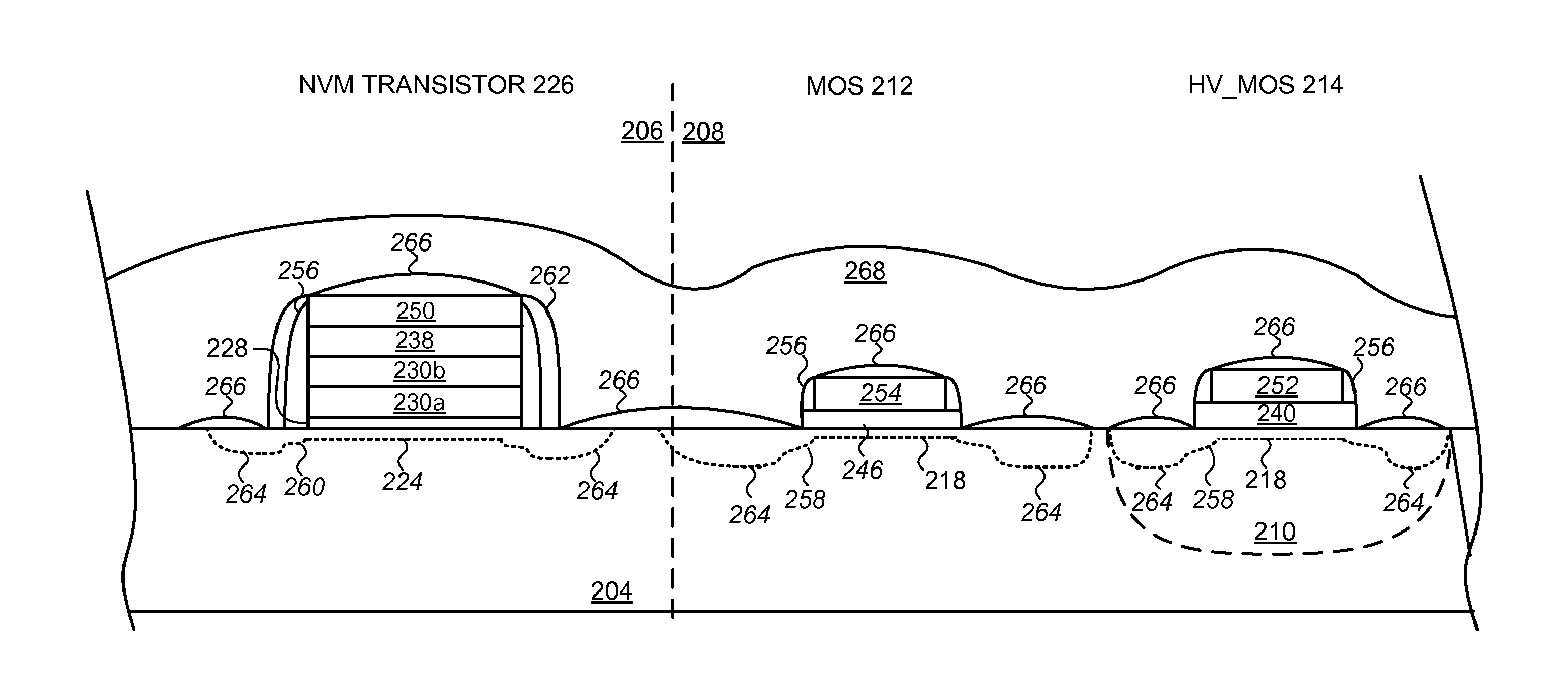
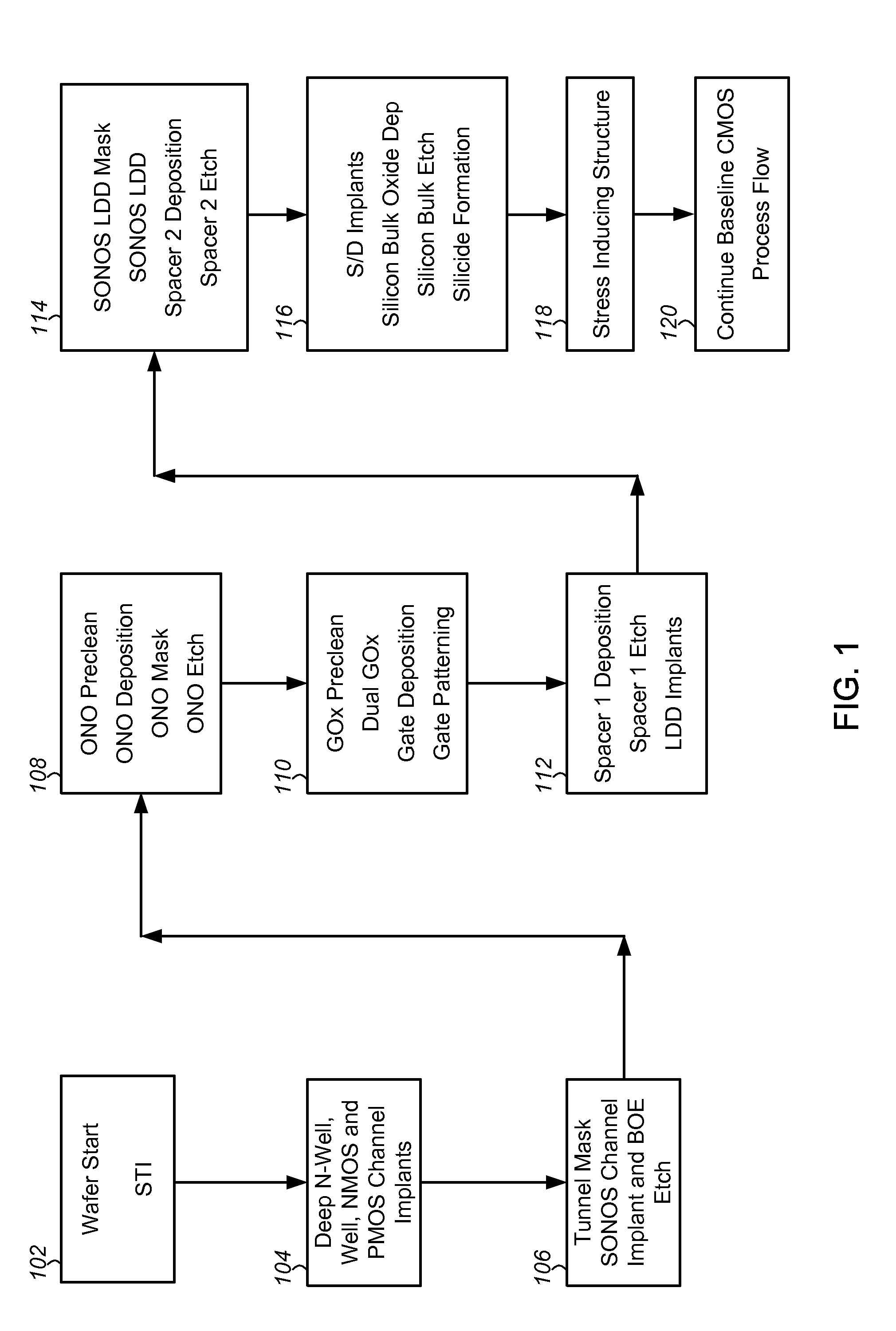
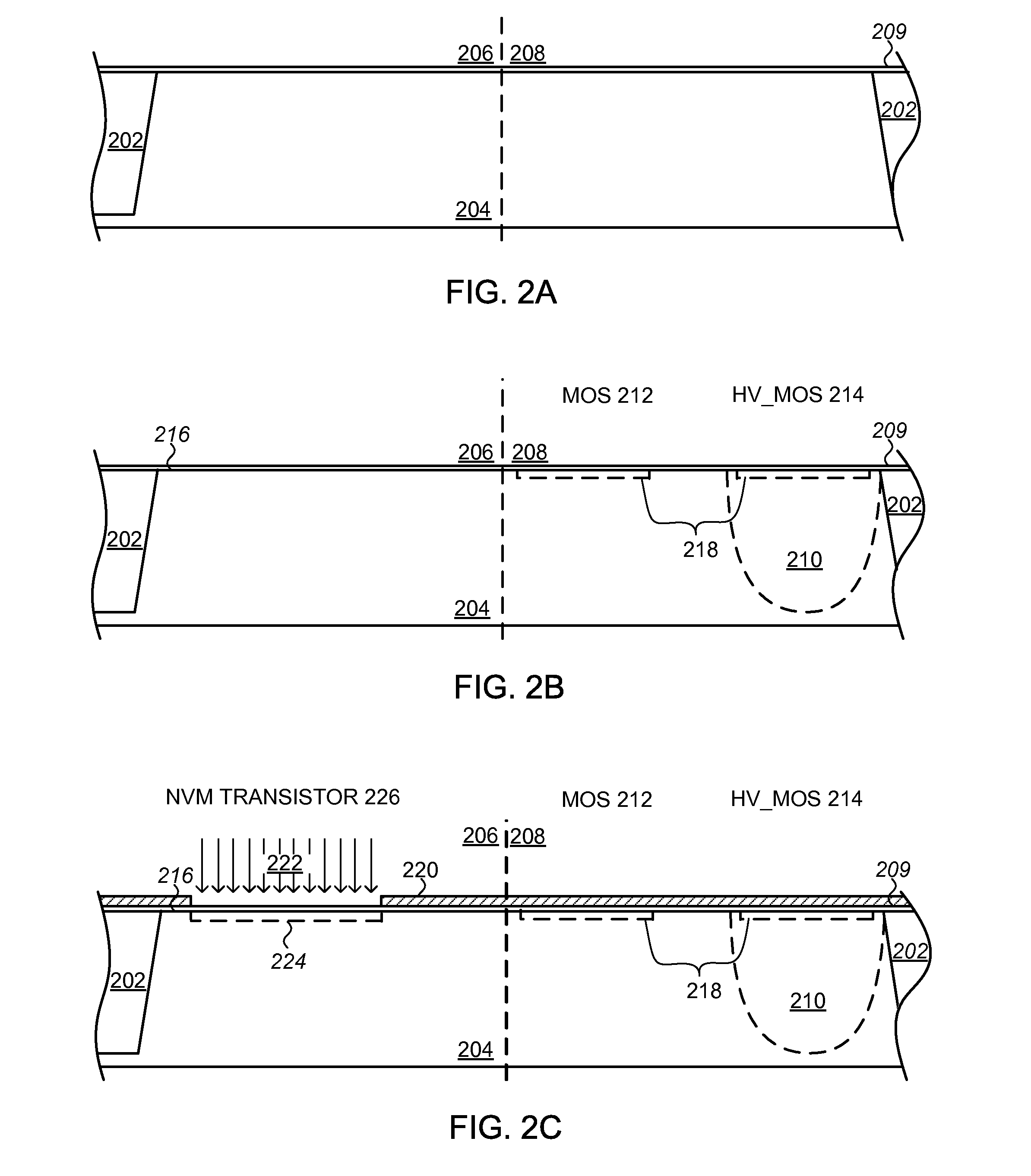
[0011]Embodiments of a memory cell including an embedded non-volatile memory (NVM) transistor and a metal-oxide-semiconductor (MOS) transistor and methods of fabricating the same are described herein with reference to figures. However, particular embodiments may be practiced without one or more of these specific details, or in combination with other known methods, materials, and apparatuses. In the following description, numerous specific details are set forth, such as specific materials, dimensions and processes parameters etc. to provide a thorough understanding of the present invention. In other instances, well-known semiconductor design and fabrication techniques have not been described in particular detail to avoid unnecessarily obscuring the present invention. Reference throughout this specification to “an embodiment” means that a particular feature, structure, material, or characteristic described in connection with the embodiment is included in at least one embodiment of the...


PUM


Abstract

Memory cells including embedded SONOS based non-volatile memory (NVM) and MOS transistors and methods of forming the same are described. Generally, the method includes: forming a dielectric stack on a substrate, the dielectric stack including a tunneling dielectric on the substrate and a charge-trapping layer on the tunneling dielectric; patterning the dielectric stack to form a gate stack of a NVM transistor of a memory device in a first region of the substrate while concurrently removing the dielectric stack from a second region of the substrate; and performing a gate oxidation process of a baseline CMOS process flow to thermally grow a gate oxide of a MOS transistor overlying the substrate in the second region while concurrently growing a blocking oxide overlying the charge-trapping layer. In one embodiment, Indium is implanted to form a channel of the NVM transistor.

Description

CROSS-REFERENCE TO RELATED APPLICATIONS[0001]This application claims the benefit of priority under 35 U.S.C. 119(e) to U.S. Provisional Patent Application Ser. No. 61 / 769,693, filed Feb. 26, 2013, and to U.S. Provisional Patent Application Ser. No. 61 / 825,196, filed May 20, 2013, both of which are incorporated by reference herein.TECHNICAL FIELD[0002]The present disclosure relates generally to semiconductor devices, and more particularly to memory cells including embedded or integrally formed SONOS based non-volatile memory (NVM) transistors and metal-oxide-semiconductor (MOS) transistors and methods for fabricating the same.BACKGROUND[0003]For many applications, such as system-on-chip, it is desirable to integrate logic devices and interface circuits based upon metal-oxide-semiconductor (MOS) field-effect transistors and non-volatile memory (NVM) transistors on a single chip or substrate. This integration can seriously impact both the MOS transistor and NVM transistor fabrication p...

Claims


Application Information

Patent Timeline
Patent Type & Authority Applications(United States)
IPC IPC(8): H01L29/66H01L29/792
CPCH01L29/66833H01L29/792H01L29/167H01L29/42348H01L29/4916H01L29/495H01L29/4966H01L29/513H01L29/517H01L29/518H10B43/40H10B43/30H01L21/823462H01L27/088H10B43/35H01L29/42344H01L29/7843
Inventor RAMKUMAR, KRISHNASWAMYKOUZNETSOV, IGOR G.PRABHAKAR, VENKATRAMAN
Owner LONGITUDE FLASH MEMORY SOLUTIONS LTD
Why Eureka
Try Eureka