Circuit device and electronic apparatus

a technology of circuit device and electronic device, which is applied in the direction of motor/generator/converter stopper, dynamo-electric converter control, pulse technique, etc., can solve the problem of fluctuation of the potential of the substrate, and achieve the effect of reducing the effect of the potential fluctuation of the substrate on the operation of the circui

Inactive Publication Date: 2014-09-04
SEIKO EPSON CORP
View PDF8 Cites 7 Cited by
  • Summary
  • Abstract
  • Description
  • Claims
  • Application Information

AI Technical Summary

Benefits of technology

[0008]An advantage of some aspects of the invention is providing a circuit device and an electronic apparatus or the like where the effect of the potential fluctuation of a substrate on the operation of a circuit can be reduced.
[0010]According to the first aspect of the invention, the second circuit constituted by the CMOS transistor is formed on the second N-type buried layer isolated from the first N-type buried layer, so that the second circuit is isolated from the P-type substrate by the second N-type buried layer. Thus, the effect of the potential fluctuation of the substrate on the circuit operation can be reduced.
[0018]With this configuration, a potential can be supplied to the P-type layer isolated from the P-type substrate via a different interconnect (first interconnect) than that for the P-type substrate. Thus, conveyance of the potential fluctuation from the P-type substrate to the P-type layer via the interconnect can be prevented or reduced.
[0029]With this configuration, the circuit that controls the first circuit or the circuit that detects the voltage or current of the first circuit can be isolated from the P-type substrate. Thus, the first circuit can be controlled precisely, or the voltage or current of the first circuit can be detected precisely.
[0031]With this configuration, even if the switching operation performed by the first circuit causes the potential of the P-type substrate to fluctuate, the effect of the switching operation on the second circuit can be prevented or reduced because the second circuit is isolated from the P-type substrate.

Problems solved by technology

Not only in a motor driver as described above, but in any circuit that performs switching operation, on / off of the current is repeated by the switching operation, and this causes a problem that the potential of a substrate fluctuates.

Method used


Image

  • Circuit device and electronic apparatus
  • Circuit device and electronic apparatus
  • Circuit device and electronic apparatus

Examples


Embodiment Construction

[0047]The following describes in detail a preferred embodiment of the invention. It should be noted that the embodiment to be described hereinafter is not intended to unduly limit the scope of the invention defined by the appended claims and that the entire configuration to be described in the embodiment is not necessarily essential as the means for achieving the invention.

[0048]1. Configuration of Substrate of Comparative Example

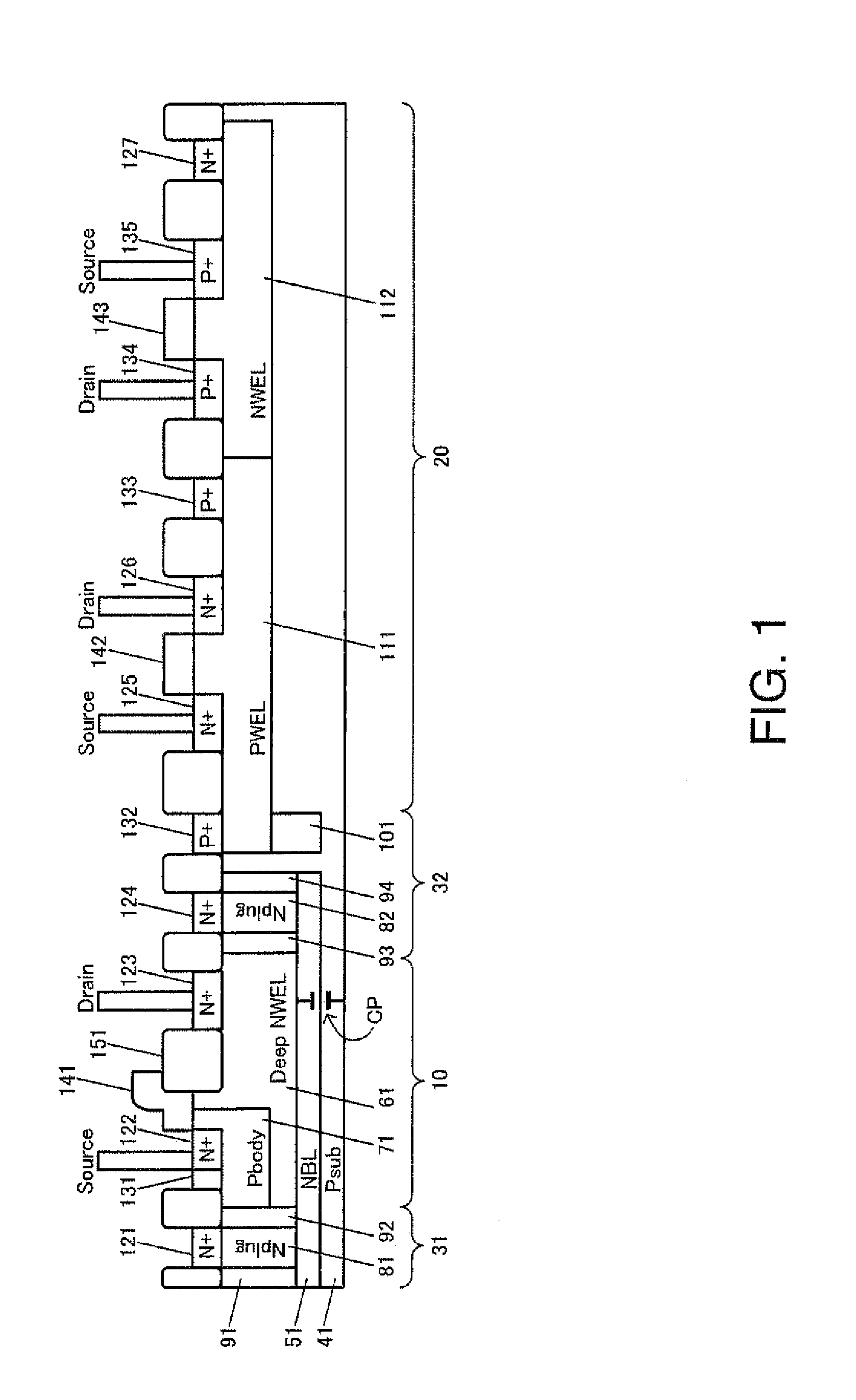
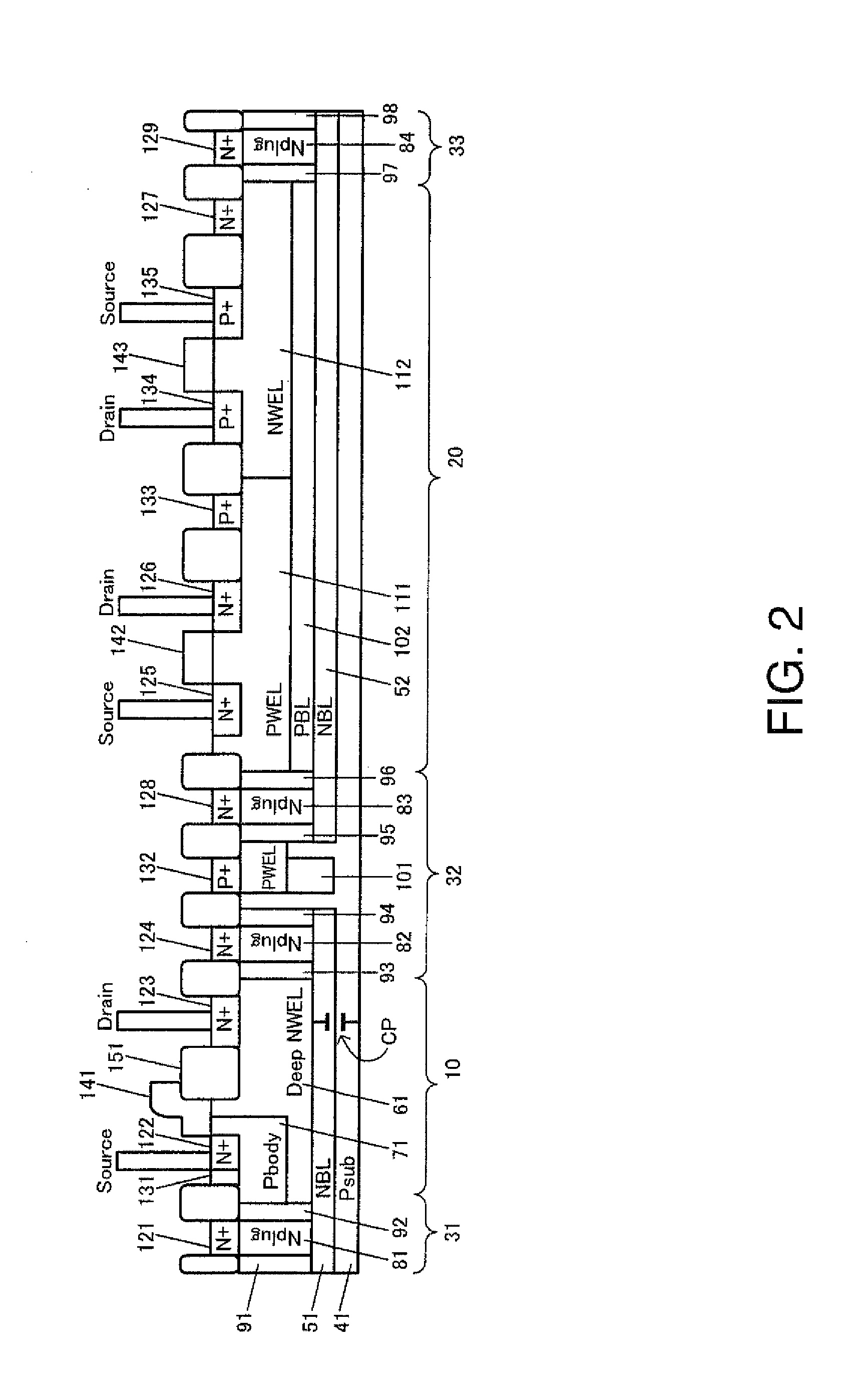
[0049]FIG. 1 shows the configuration of a substrate of a comparative example of this embodiment. FIG. 1 is a cross-sectional view of a substrate of an integrated circuit device constituting a circuit device.

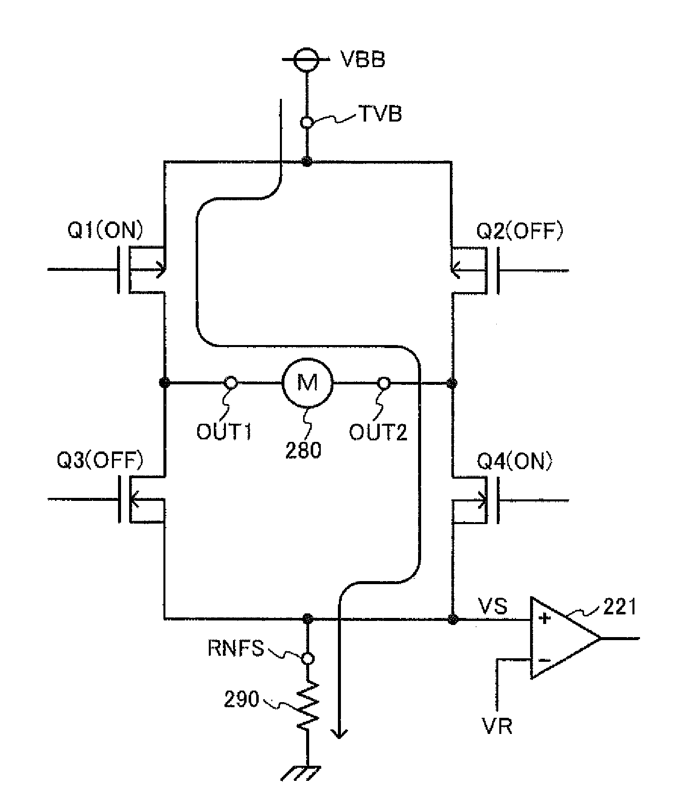
[0050]It should be noted that although a case where the circuit device is a motor driver as described later with reference to FIG. 3, for example, will be described as an example below, this embodiment is not limited to this, but can be applied to various types of circuit devices that perform switching operation of a drive current or a drive voltage. For...


PUM


Abstract

An electronic circuit includes a noise source and an analog circuit and a logic circuit that may be adversely affected by noise. At least a portion of the analog circuit and the logic circuit is formed on a buried impurity layer whose conductivity is different from that of a substrate, and at least a portion of the periphery of that portion is surrounded by an impurity layer that is different from the substrate. Thus, propagation of the noise from the noise source is prevented.

Description

BACKGROUND[0001]1. Technical Field[0002]The present invention relates to a circuit device and an electronic apparatus or the like.[0003]2. Related Art[0004]A technique of controlling the number of revolutions of a motor by controlling a chopping current is known as a technique for a motor driver that drives a DC motor. In this technique, a current flowing to a bridge circuit is converted to a voltage by a sense resistor, and the resultant voltage is compared with a reference voltage, to detect a chopping current. The detection result is fed back to a control circuit, to perform PWM control of a drive signal for the bridge circuit, thereby rotating a motor at a fixed rate.[0005]For example, JP-A-2008-042975 discloses a technique of improving the precision of detection of the chopping current in such a motor driver. In this technique, a sense resistor is provided for each half bridge of an H-bridge, where one resistor detects that the current in the charge period has reached a predete...

Claims


Application Information

Patent Timeline
Patent Type & Authority Applications(United States)
IPC IPC(8): H02P6/00H01L27/092H03K17/687H01L21/336H01L21/822H01L21/8238H01L27/04H01L29/78
CPCH02P6/001H03K17/687H01L27/092H01L21/823814H01L21/82385H01L21/823878H01L21/823892H01L21/761H03K17/0822H03K2217/0027H03K2217/0045H02M7/53871H01L29/7816H01L29/7835H01L27/0928H01L29/0646
Inventor MORIYA, ISAMUYAMADA, ATSUSHI
Owner SEIKO EPSON CORP
Why Eureka
Try Eureka