Method and apparatus for enhancing channel strain

a channel strain and strain technology, applied in the direction of electrical equipment, basic electric elements, semiconductor devices, etc., can solve the problems of affecting the level of channel strain obtained so far, affecting the level of channel strain, and affecting the quality of the channel strain

Active Publication Date: 2014-09-04
TAIWAN SEMICON MFG CO LTD
View PDF3 Cites 20 Cited by
  • Summary
  • Abstract
  • Description
  • Claims
  • Application Information

AI Technical Summary

Benefits of technology

[0006]According to another of the broader forms of the invention, an apparatus includes a substrate, first and second projections extending upwardly from the substrate, the first projection having a tensile-strained first channel region therein and the second projection having a compression-strained second channel region therein, and first and second gate structures engaging the first and second projections adjacent to the first and second channel regions, respectiv

Problems solved by technology

As the semiconductor industry has strived for higher device density, higher performance, and lower costs, problems involving both fabrication and design have been encountered.
However, this scaling-down trend has slowed due to physical limits of IC materials.
Res

Method used


Image

  • Method and apparatus for enhancing channel strain
  • Method and apparatus for enhancing channel strain
  • Method and apparatus for enhancing channel strain

Examples


Embodiment Construction

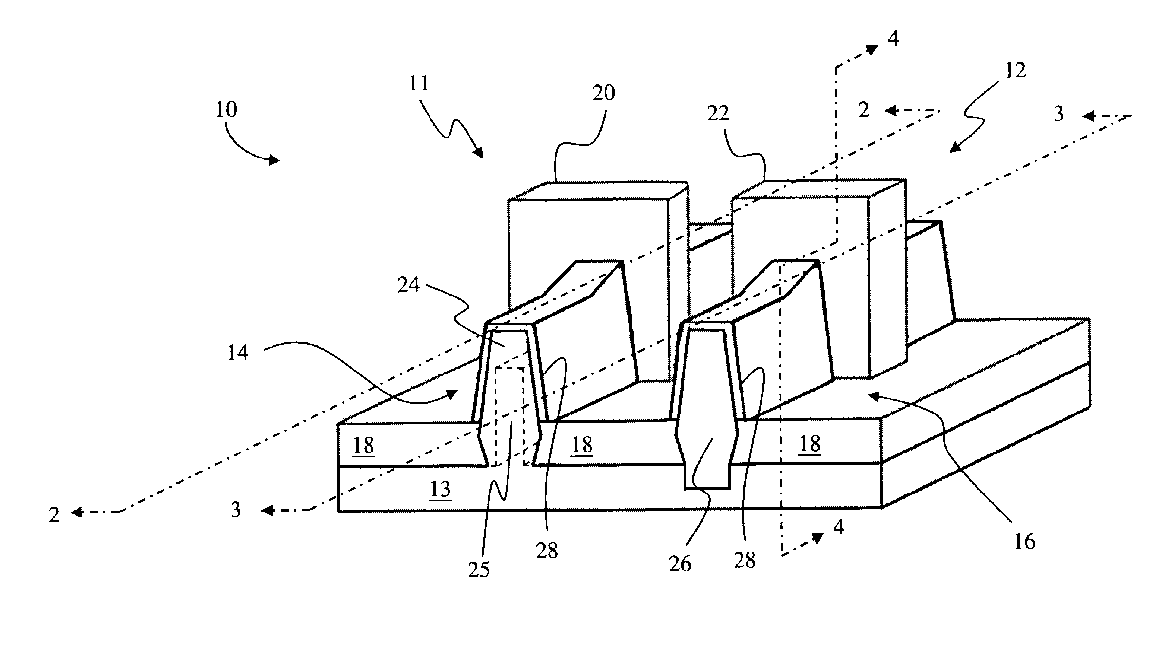
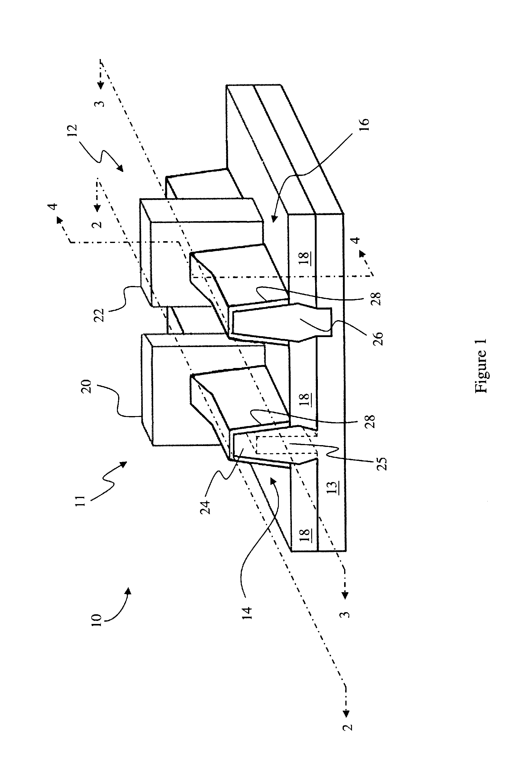
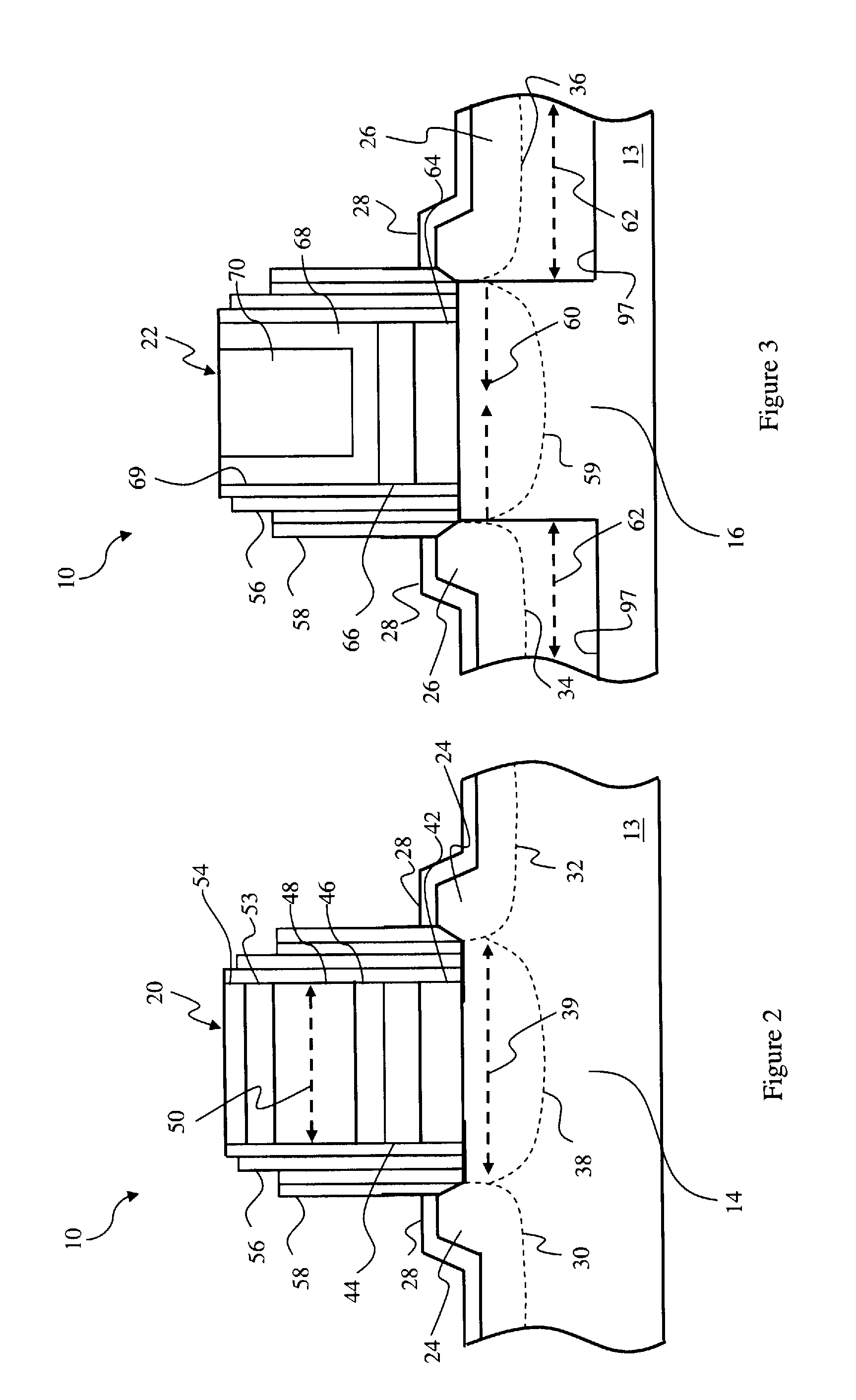
[0015]The present disclosure relates generally to semiconductor devices and more particularly, to a FinFET device and method of fabricating a FinFET device or portion of a device. It is understood, however, that specific embodiments are provided as examples to teach the broader inventive concept, and one of ordinary skill in the art can easily apply the teaching of the present disclosure to other methods or apparatus. In addition, it is understood that the methods and apparatus discussed in the present disclosure include some conventional structures and / or processes. Since these structures and processes are well known in the art, they will only be discussed in a general level of detail. Furthermore, reference numbers are repeated throughout the drawings for sake of convenience and example, and such repetition does not indicate any required combination of features or steps throughout the drawings. Moreover, the formation of a first feature over and on a second feature in the descript...


PUM


Abstract

An apparatus includes a substrate having a strained channel region, a dielectric layer over the channel region, first and second conductive layers over the dielectric layer having a characteristic with a first value, and a strain-inducing conductive layer between the conductive layers having the characteristic with a second value different from the first value. A different aspect involves an apparatus that includes a substrate, first and second projections extending from the substrate, the first projection having a tensile-strained first channel region and the second projection having a compression-strained second channel region, and first and second gate structures engaging the first and second projections, respectively. The first gate structure includes a dielectric layer, first and second conductive layers over the dielectric layer, and a strain-inducing conductive layer between the conductive layers. The second gate structure includes a high-k dielectric layer adjacent the second channel region, and a metal layer.

Description

PRIORITY DATA[0001]This application is a divisional of U.S. application Ser. No. 12 / 780,124, filed on May 14, 2010, entitled “Method and Apparatus for Enhancing Channel Strain,” the entirety of which is hereby incorporated by reference.BACKGROUND[0002]As the semiconductor industry has strived for higher device density, higher performance, and lower costs, problems involving both fabrication and design have been encountered. One solution to these problems has been the development of a fin-like field effect transistor (FinFET). A typical FinFET includes a thin vertical ‘fin’ formed by etching spaced recesses into a substrate. The source, drain, and channel regions are defined within this fin. The transistor's gate is wrapped around the channel region of the fin, engaging it on both the top of the fin and the sides of the fin. This configuration allows the gate to induce current flow in the channel from three sides. Thus, FinFET devices have the benefit of higher current flow and reduc...

Claims


Application Information

Patent Timeline
IPC IPC(8): H01L29/66H01L21/02
CPCH01L21/02664H01L29/66795H01L21/823807H01L21/823821H01L21/845H01L27/0924H01L27/1211H01L29/165H01L29/66545H01L29/66636H01L29/7848H01L29/7847H01L29/511H01L21/823814H01L21/02532H01L21/324
Inventor CHENG, MING-LUNGLIN, YEN-CHUNLIN, DA-WEN
Owner TAIWAN SEMICON MFG CO LTD
Why Eureka
Try Eureka