
Pa cell, pa module, wireless communication unit, RF transmitter architecture and method therefor

a technology of rf transmitter and power amplifier, which is applied in the direction of power amplifier, transmitter/receiver shaping network, high frequency amplifier, etc., can solve the problems of low power efficiency of such conventional rf transmitter, noise shaping techniques are often required, and analog circuits do not scale particularly well, so as to achieve the effect of alleviating one or two, and reducing the number o

Active Publication Date: 2014-09-11
MEDIATEK SINGAPORE PTE LTD SINGAPORE
View PDF13 Cites 15 Cited by
  • Summary
  • Abstract
  • Description
  • Claims
  • Application Information

AI Technical Summary

Benefits of technology

The invention aims to reduce the size of power amplifiers by using a single array of cells that can be controlled in both in-phase and quadrature, instead of two separate arrays. This results in a more efficient use of silicon area, allowing for a more compact power amplifier.

Problems solved by technology

However, it is known that analogue circuits do not scale particularly well with the deep sub-micron CMOS process.
Furthermore, a large number of conventional RF transmitters use linear power amplifiers.
Accordingly, the power efficiency of such conventional RF transmitters is usually very low, due to the low efficiency of the linear PAs used therein.
Furthermore, in order to meet stringent co-existence requirements of various wireless standards, noise shaping techniques are often required.
However, a problem with these known transmitter designs is that, due to the inherent bandwidth expansion characteristics of the AM (amplitude modulation) and PM (phase modulation) signals in a polar architecture, they are only suitable for narrowband modulated signals.
However, a problem with such hybrid polar transmitters is that they suffer from both amplitude and phase quantization noise, thus requiring significant noise shaping.
However, such transmitter designs require a linear PA, and direct I / Q RF digital-to-analogue conversion is less power efficient than a digital polar transmitter design.
However, this design still comprises a generally conventional architecture, and so PA efficiency is low.
However, digital algorithms are limited by the availability of circuit speed; therefore finding simple and effective digital algorithms is crucial from an implementation perspective.
However, such clock frequencies are, in a practical CMOS and / or subscriber communication unit sense, not implementable.

Method used


Image

  • Pa cell, pa module, wireless communication unit, RF transmitter architecture and method therefor
  • Pa cell, pa module, wireless communication unit, RF transmitter architecture and method therefor
  • Pa cell, pa module, wireless communication unit, RF transmitter architecture and method therefor

Examples


Embodiment Construction

[0062]The present invention will now be described with reference to an example of a radio frequency (RF) transmitter architecture for use within, say, a wireless telecommunication handset and adapted in accordance with some embodiments of the present invention. However, it will be appreciated that the inventive concept described herein is not limited to specific features of the illustrated example, and may equally be implemented within alternative applications.

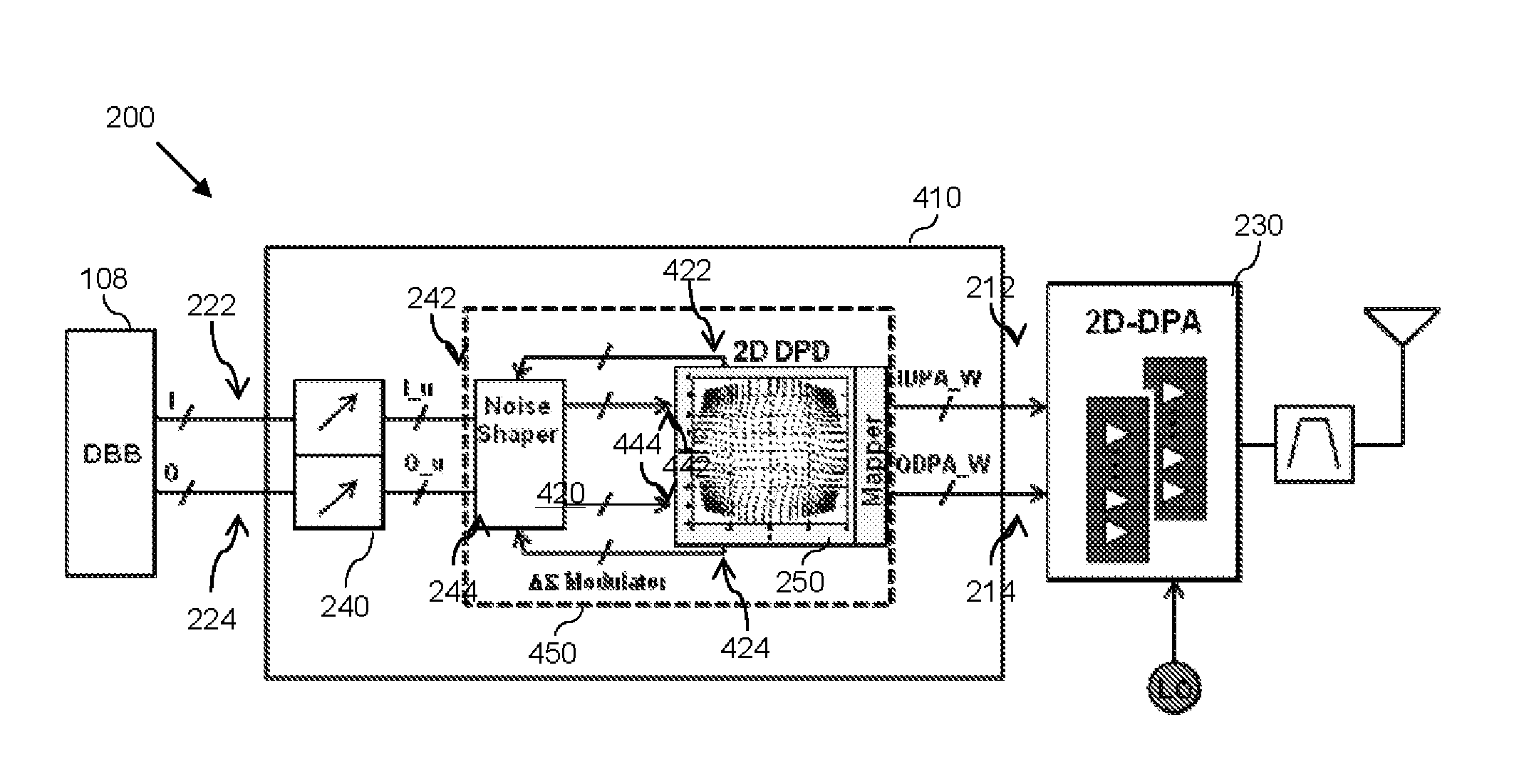
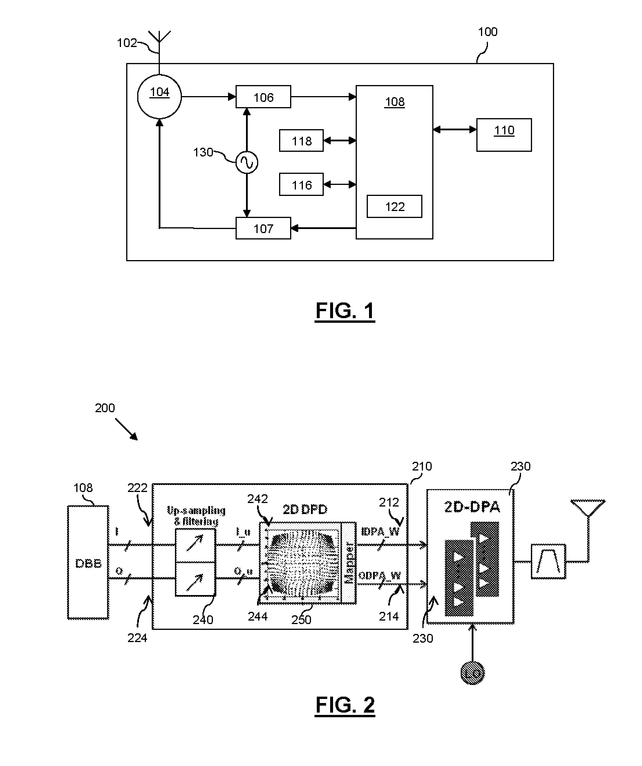
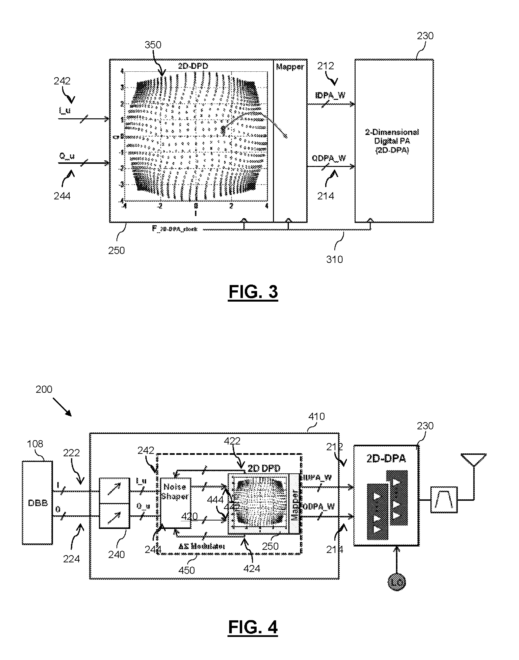
[0063]Referring first to FIG. 1, there is illustrated an example of a simplified block diagram of part of an electronic device 100 adapted to support the inventive concept of an example of the present invention. The electronic device 100, in the context of the illustrated embodiment of the invention, is a wireless telecommunication handset. As such, the electronic device 100 comprises an antenna 102 and contains a variety of well known radio frequency transceiver components or circuits operably coupled to the antenna 102. In p...


PUM


Abstract

A power amplifier cell includes a first input arranged to receive an in-phase control signal, a second input arranged to receive a quadrature control signal, an input stage arranged to output a drive signal based at least partly on the received in-phase and quadrature control signals, and an output stage arranged to receive at an input thereof the drive signal output by the input stage, and to generate an output signal for the power amplifier cell in response to the received drive signal.

Description

CROSS REFERENCE TO RELATED APPLICATIONS[0001]This is a continuation-in-part (CIP) of co-pending U.S. application Ser. No. 13 / 298,282 (filed on Nov. 16, 2011), which claims the benefit of U.S. provisional application No. 61 / 477,684 (filed on Apr. 21, 2011) and U.S. provisional application No. 61 / 500,900 (filed on Jun. 24, 2011); and claims the benefit of U.S. provisional application No. 61 / 825,628 (filed on May 21, 2013). The entire contents of the related applications are incorporated herein by reference.BACKGROUND[0002]The field of this invention relates to a power amplifier cell, a power amplifier module, a wireless communication unit, a radio frequency transmitter architecture and a method of performing digital pre-distortion calibration within a radio frequency architecture.[0003]Advances in the deep sub-micron CMOS (Complimentary Metal-Oxide Semiconductor) process have lead to digital circuits becoming smaller and more power efficient. However, it is known that analogue circuit...

Claims


Application Information

Patent Timeline
IPC IPC(8): H04L25/03H03F3/24H03F3/217H03F1/32H03F3/19
CPCH04L25/03343H03F1/3247H03F1/3205H03F3/19H03F3/2175H03F2203/21193H04L25/0328H03F2200/451H03F2201/3227H03F2201/3233H03F3/245H04B1/0475H04L27/367H04B2001/0425H03F1/3241
Inventor DENG, ZHIMINGPENG, CHUN-HSIEN
Owner MEDIATEK SINGAPORE PTE LTD SINGAPORE
Learn More