Image processing apparatus, imaging apparatus, image processing method, and program

Active Publication Date: 2014-09-18
SONY SEMICON SOLUTIONS CORP
View PDF4 Cites 55 Cited by
  • Summary
  • Abstract
  • Description
  • Claims
  • Application Information

AI Technical Summary

Benefits of technology

[0050]According to one embodiment of the present disclosure, an apparatus and a method that can efficiently generate a wide dynamic range image to which each pixel information of a high sensitivity pixel and a low sensitivity pixel is applied are realized.
[0051]Specifically, high sensitivity pixel information obtained by adding pixel values of a plurality of high sensitivity pixels and low sensitivity pixel information obtained by adding pixel values of a plurality of low sensitivity pixels are output as output pixel signals from pixels of different sensitivities from a pixel unit, these pixel information are combined in a pixel information combining unit, an output pixel value is determined, and an output image of a wide dynamic range is output. In the pixel information combining unit,

Problems solved by technology

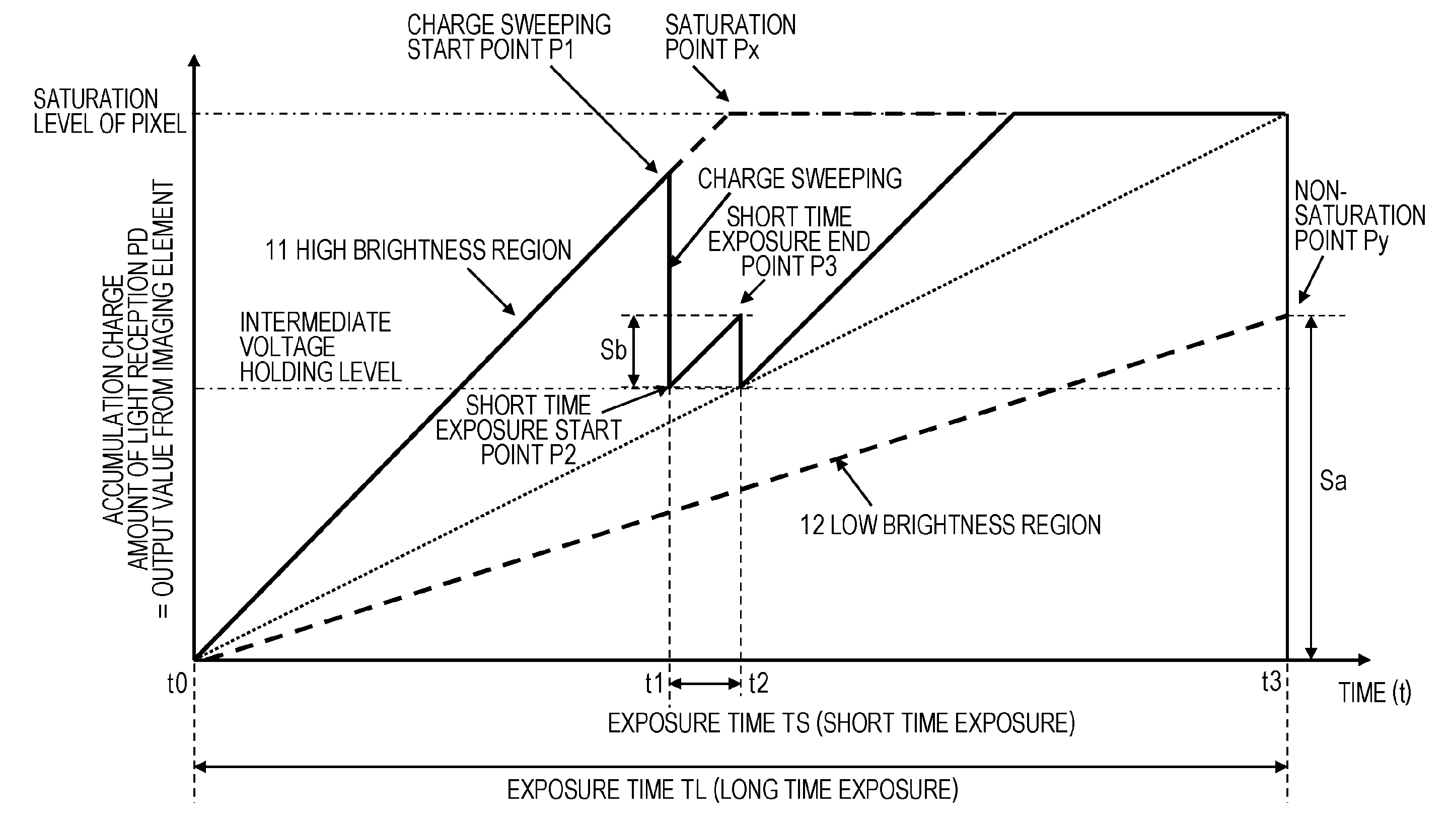
However, there is an upper limit in a charge accumulation amount in a photoelectric conversion element.
However, if the shutter is released fast in imaging of a subject in which a bright place and a dark place are mixed, a sufficient exposure time is not taken in a dark portion.
As a result, pixe

Method used


Image

  • Image processing apparatus, imaging apparatus, image processing method, and program
  • Image processing apparatus, imaging apparatus, image processing method, and program
  • Image processing apparatus, imaging apparatus, image processing method, and program

Examples


second embodiment

(3.1. Second Embodiment)

[0228]In the embodiment described above, as the circuit configuration of each pixel, all of the pixels have the same circuit configuration, as described with reference to FIG. 6. Specifically, the circuit configuration is a circuit configuration in which each transistor of a control transistor (T1), an amplifying transistor (AMP), a reset transistor (RST), and a selection transistor (SEL) is set in each pixel unit.

[0229]However, for each transistor, a configuration in which partial transistors are used commonly to a plurality of pixels as one setting is enabled.

[0230]An example will be described with reference to FIG. 13.

[0231]A pixel unit configuration illustrated in FIG. 13 is a configuration in which the AMP transistor, the RST transistor, and the SEL transistor are shared by the pixels in which these transistors are arranged in four columns as one setting. FIG. 13 is a diagram illustrating an example of a pixel array based on a sharing pixel structure.

[02...

third embodiment

(3-2. Third Embodiment)

[0268]Next, another example of the pixel unit configuration in which the transistors are shared by the plurality of pixels, similar to the second embodiment, will be described as a third embodiment with reference to FIG. 17 and the following drawings.

[0269]A pixel unit configuration according to the third embodiment illustrated in FIG. 17 is a transistor sharing configuration in which three transistors of an amplifying transistor (AMP), a reset transistor (RST), and a selection transistor (SEL) are realized as one setting in a unit of a pixel block including eight pixels of four high sensitivity pixels of a high sensitivity pixel column and four low sensitivity pixels of a low sensitivity pixel column.

[0270]A pixel block 351 illustrated in FIG. 17(a) is a pixel block including eight pixels of four high sensitivity pixels of a high sensitivity pixel column and four low sensitivity pixels of a low sensitivity pixel column and a circuit configuration of the pixel...

fourth embodiment

(3-3. Fourth Embodiment)

[0312]Next, an embodiment in which a gradation converter 401 is configured at the back of a pixel information combining unit 162 of an operation unit 160 of an imaging device 102 as illustrated in FIG. 21 will be described as a fourth embodiment of the present invention.

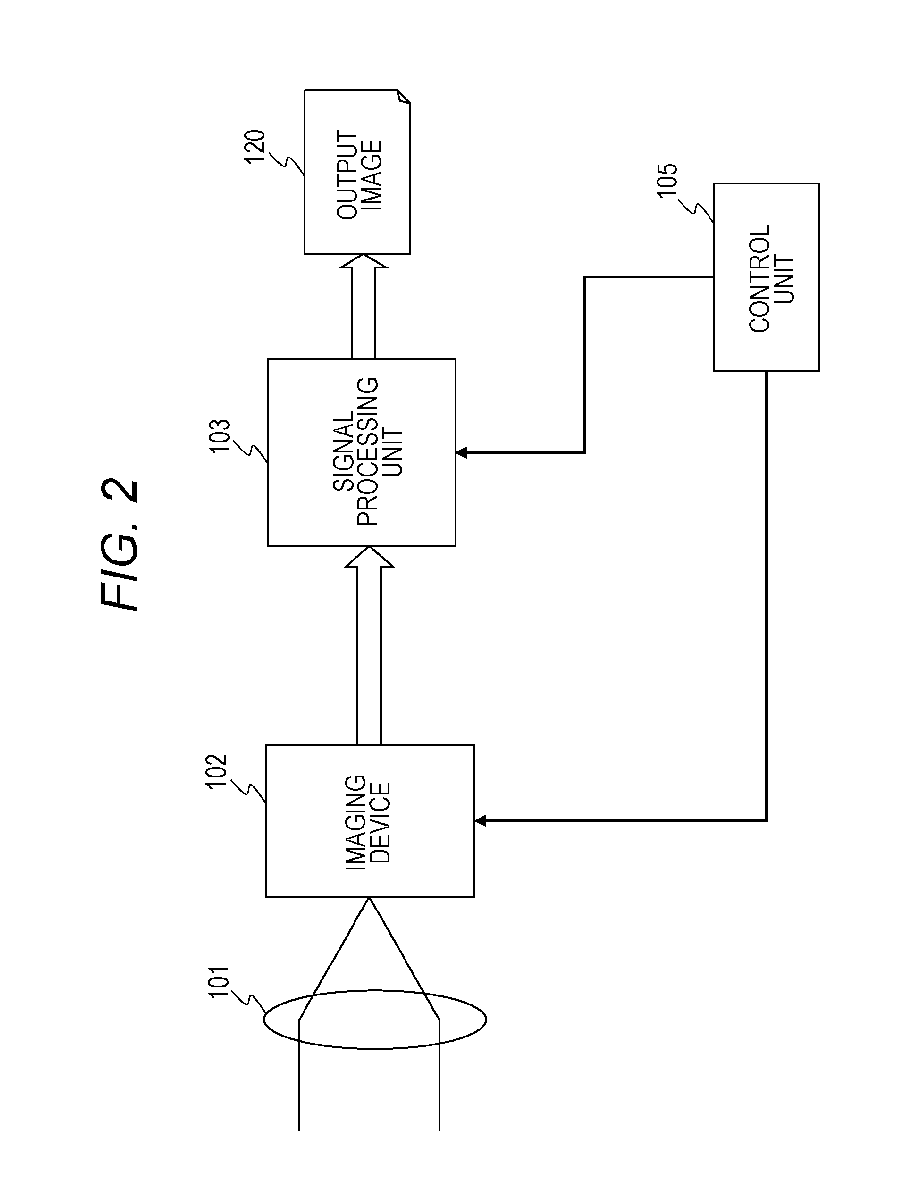
[0313]FIG. 21 is a diagram illustrating a configuration of the imaging device 102 according to the fourth embodiment. The configuration illustrated in FIG. 21 is a configuration in which the gradation converter 402 is provided at the back of the pixel information combining unit 162 of the operation unit 160 of the imaging device 102, which is described above as the first embodiment and is illustrated in FIG. 3. The other configuration is the same as the configuration of the first embodiment illustrated in FIG. 3. An entire configuration of an imaging processing apparatus (imaging apparatus) is the same as the configuration described above with reference to FIG. 2, similar to the first embodime...


PUM


Abstract

An apparatus and a method that can efficiently generate a wide dynamic range image to which each piece of pixel information of a high sensitivity pixel and a low sensitivity pixel is applied are realized. High sensitivity pixel information obtained by adding pixel values of a plurality of high sensitivity pixels and low sensitivity pixel information obtained by adding pixel values of a plurality of low sensitivity pixels are output as output pixel signals from pixels of different sensitivities from a pixel unit, these pixel information are combined in a pixel information combining unit, an output pixel value is determined, and an output image of a wide dynamic range is output. In the pixel information combining unit, a weight for the high sensitivity pixel information or the low sensitivity pixel information is changed according to brightness of a subject, weight addition of the high sensitivity pixel information and the low sensitivity pixel information is performed, a pixel value of an output image is determined, and the pixel value is output.

Description

TECHNICAL FIELD[0001]The present disclosure relates to an image processing apparatus, an imaging apparatus, an image processing method, and a program. In detail, the present disclosure relates to an image processing apparatus, an imaging apparatus, an image processing method, and a program that enable an image of a wide dynamic range to be generated.BACKGROUND ART[0002]Solid-state imaging devices such as a CCD image sensor or a complementary metal oxide semiconductor (CMOS) image sensor that are used in a video camera or a digital still camera perform photoelectric conversion for accumulating a charge according to an amount of incident light and outputting an electric signal corresponding to the accumulated charge. However, there is an upper limit in a charge accumulation amount in a photoelectric conversion element. If light of an amount equal to or more than a constant amount is received, so-called overexposure in which an accumulation charge amount reaches a saturation level and ...

Claims


Application Information

Patent Timeline
IPC IPC(8): H04N5/235
CPCH04N5/2352H04N5/2355H01L27/14609H01L27/14647H04N23/73H04N25/589H04N25/70H04N25/778H04N23/84H04N25/134H04N23/741H04N23/72
Inventor KASAI, MASANORIASAYAMA, GO
Owner SONY SEMICON SOLUTIONS CORP
Why Eureka
Try Eureka