
High throughput multi-layer stack deposition

a multi-layer, high-throughput technology, applied in the direction of coatings, chemical vapor deposition coatings, metallic material coating processes, etc., can solve the problems of non-uniformity, non-uniform performance, and increase the likelihood of non-uniformity, and achieve the effect of high-throughput multi-layer stack formation

Inactive Publication Date: 2014-09-25
APPLIED MATERIALS INC
View PDF9 Cites 1 Cited by
  • Summary
  • Abstract
  • Description
  • Claims
  • Application Information

AI Technical Summary

Benefits of technology

This patent describes an apparatus and method for forming multi-layer stacks on a substrate at high rates. The apparatus includes a substrate support, a processing chamber, and two precursor mixture flow paths. The method involves flowing precursor mixtures through the flow paths, forming a plasma by coupling RF power to the mixtures, and using a diverter to direct the first precursor to the chamber where the first film is formed. Additionally, a third precursor mixture is flowed to the chamber where a second film is formed. The compounds in the precursor mixtures are selected to avoid spontaneous reactions. The technical effect of this invention is the ability to rapidly form multi-layer stacks on substrates with high efficiency.

Problems solved by technology

Uniformity in processing conditions has always been important to semiconductor manufacturing, and as critical dimensions of devices continue to shrink the need for precision increases, and as substrate size increases, the likelihood of non-uniformity increases.
Non-uniformity arises from numerous causes, which may be related to device properties, equipment features, and the chemistry and physics of fabrication processes.
The electrical properties of such devices depend on the thickness and composition of the various layers, so non-uniformity in the thickness and / or composition of the layers leads to non-uniformity in performance.
Non-uniformity within a single device can render the device inoperative, and non-uniformity from device to device leads to different devices having different electrical properties, sometimes substantially different.

Method used


Image

  • High throughput multi-layer stack deposition
  • High throughput multi-layer stack deposition

Examples


Embodiment Construction

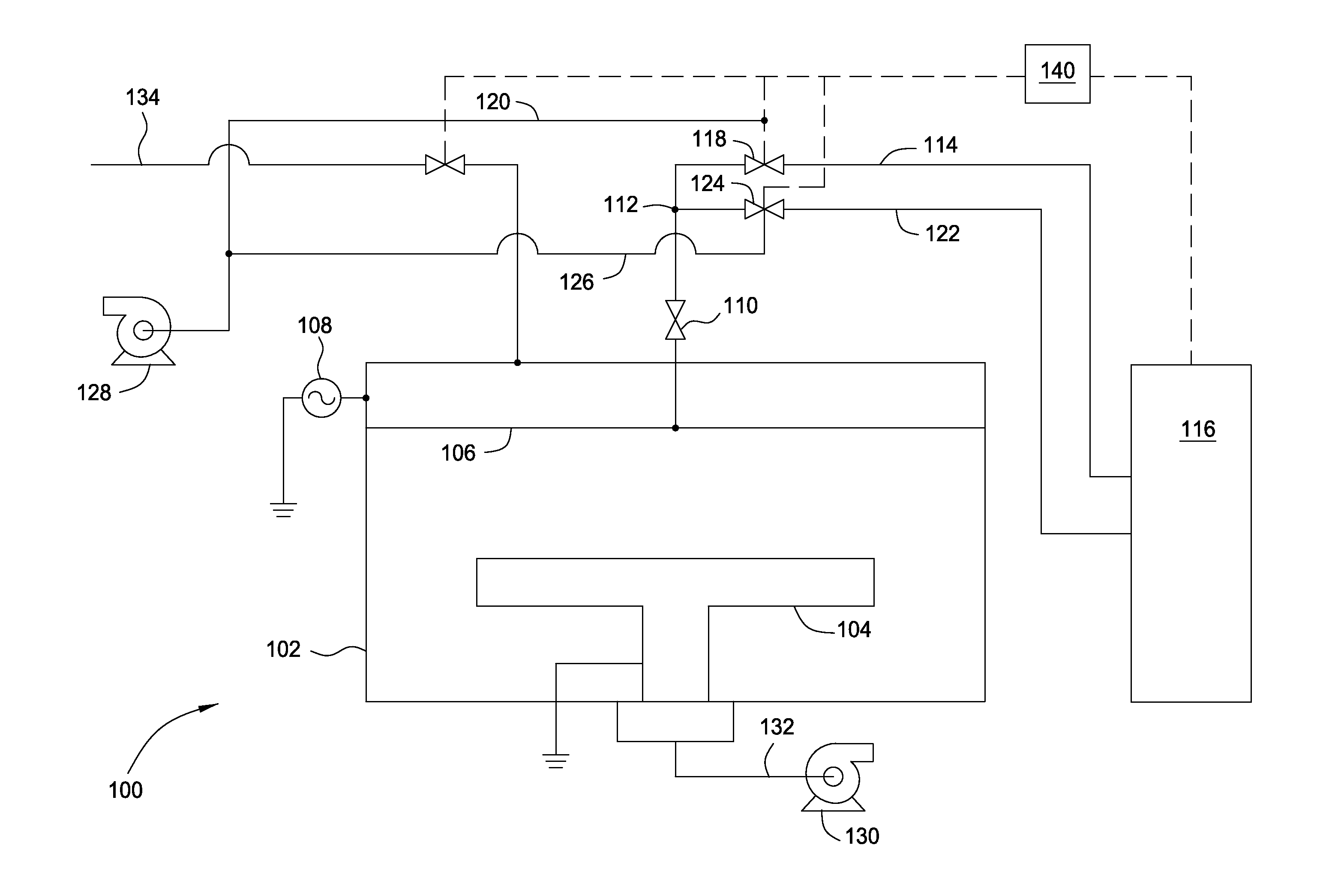
[0013]Apparatus and methods are described for forming multi-layer stacks on semiconductor substrates. Plasma processing is used to form each layer of the stack, and the process is transitioned from forming a first layer to forming a second layer while maintaining the plasma and minimizing cross-contamination between the two layers. Precursor lines are coupled to a processing chamber for delivering precursor gas mixtures to the chamber. Each precursor line has a diverter located close to the processing chamber to facilitate switching of precursors with minimal cross-contamination. A separate exhaust system is provided for the processing chamber and for the divert lines.

[0014]FIG. 1 is a schematic side view of an apparatus 100 according to one embodiment. A processing chamber 102 contains a substrate support 104 and a lid assembly 106 opposite the substrate support 104. The lid assembly 106 may be, or may contain, an electrode coupled to a source of plasma power 108, which may be an R...


PUM

PropertyMeasurementUnit
frequencyaaaaaaaaaa
semiconductoraaaaaaaaaa
plasma poweraaaaaaaaaa

Abstract

Methods and apparatus for high rate formation of multi-layer stacks on semiconductor substrate is provided. A chamber for forming such stacks at high rates includes a first precursor line and a second precursor line. The first precursor line is coupled to a first diverter, which is coupled to a gas inlet in a lid assembly of the chamber. The second precursor line is coupled to a second diverter, which is also coupled to the gas inlet. The first diverter is also coupled to a first divert line, and the second diverter is coupled to a second divert line. Each of the first and second divert lines is coupled to a divert exhaust system. A chamber exhaust system is coupled to the chamber. The diverters are typically located close to the lid assembly.

Description

CROSS-REFERENCE TO RELATED APPLICATIONS[0001]This application claims benefit of U.S. Provisional Patent Application Ser. No. 61 / 804,017 filed Mar. 21, 2013, which is incorporated herein by reference.FIELD[0002]Embodiments of the present invention generally relate to semiconductor manufacturing apparatus and methods. Specifically, embodiments described herein relate to chemical vapor deposition chambers having high rate deposition features.BACKGROUND[0003]For over 50 years, the number of transistors formed on an integrated circuit has doubled approximately every two years. This two-year-doubling trend, also known as Moore's Law, is projected to continue, with devices formed on semiconductor chips shrinking from the current critical dimension of 20-30 nm to below 100 Angstroms in future fabrication processes currently being designed. As device geometries shrink, substrate sizes also grow. As the 300 mm wafer replaced the 200 mm wafer years ago, the 300 mm wafer may be replaced by the ...

Claims


Application Information

Patent Timeline
Patent Type & Authority Applications(United States)
IPC IPC(8): H01L21/02
CPCH01L21/02274H01L21/02211H01L21/0217H01L21/02164C23C16/345C23C16/402C23C16/45523C23C16/45561C23C16/509H01L21/022
Inventor HAN, XINHAIJIANG, ZHIJUNRAJAGOPALAN, NAGARAJANKIM, BOK HOENSANKARAKRISHNAN, RAMPRAKASHBALASUBRAMANIAN, GANESHROCHA- ALVAREZ, JUAN CARLOSSRINIVASAN, MUKUND
Owner APPLIED MATERIALS INC
Learn More