Articles and methods for rapid manufacturing of solid state light sources

a technology of solid-state light sources and manufacturing methods, applied in semiconductor/solid-state device manufacturing, semiconductor devices, electrical devices, etc., can solve the problems of low thermal conductivity, low cost, and fundamental limitation of all organic based materials, so as to reduce overall cost and reduce manufacturing costs

Inactive Publication Date: 2014-10-09
GOLDENEYE
View PDF3 Cites 23 Cited by
  • Summary
  • Abstract
  • Description
  • Claims
  • Application Information

AI Technical Summary

Benefits of technology

[0005]Fiber lasers can be over 50% efficient from an electrical to optical conversion standpoint. Fiber lasers also allow for very controlled placement of the energy onto a surface or within a volume and ease of integration into production processes. Conventional sintering and melt fusing requires that the entire assembly is heated to the sintering temperature. The ability to very precisely deliver a high energy input rapidly into a specific region of an assembly is critical to prevent unnecessary thermal stressing of LEDs and other temperature sensitive parts. As previously disclosed by the present inventors (for example, in LEDs can be integrated into thermally conductive luminescent elements to make high powered packages and self cooling light sources. Fiber lasers can also deliver a beam quality approaching the diffraction limit which allows for very precise spot sizes. Beam shaping including flat tops are also possible either with a secondary optic or shaped fiber.
[0007]This specification discloses methods and articles based on fiber laser processing that limits the amount and duration of heating that the LEDs are exposed to during bonding, interconnect formation, and packaging. In particular, methods of sintering and fusing inorganic materials such as, but not limited to, silver conductive inks, ceramic powders and glasses, as well as composites made from these materials, can use fiber laser based systems. While other laser systems are anticipated, fiber lasers are preferred based on their higher efficiency, reliability, low cost per watt and output wattage.
[0009]Fiber lasers can also be used in laser liftoff applications. In particular, a fiber laser based system creates a narrow line pattern (less than 10 microns wide×greater than 100 micron wide) coupled to a galvo for laser liftoff of nitride foils from nitride templates (typically grown of sapphire). An interconnect means laser fuses conductive inks to contact surfaces on LED and external interconnects, thereby reducing the thermal heating of the LED itself while allowing for the use inorganic binders in the conductive inks.
[0011]By embedding LED in solid luminescent elements rapid fabrication techniques can be used, which dramatically reduce overall cost. The solid luminescent element enables the incorporation of electrical interconnects which are robust enough for high speed processes like laser soldering. Fiber lasers also can be used to form the solid luminescent element, to cut pockets in the solid luminescent element, and to dice the solid luminescent element. All these processes reduce the cost of manufacturing of the overall light sources.

Problems solved by technology

This is a fundamental limitation of all organic based materials.
The organic materials also suffer from low thermal conductivity and low thermal stability.
Unfortunately, inorganic materials tend to be processed at elevated temperatures which are detrimental to LEDs.

Method used


Image

  • Articles and methods for rapid manufacturing of solid state light sources
  • Articles and methods for rapid manufacturing of solid state light sources
  • Articles and methods for rapid manufacturing of solid state light sources

Examples


Embodiment Construction

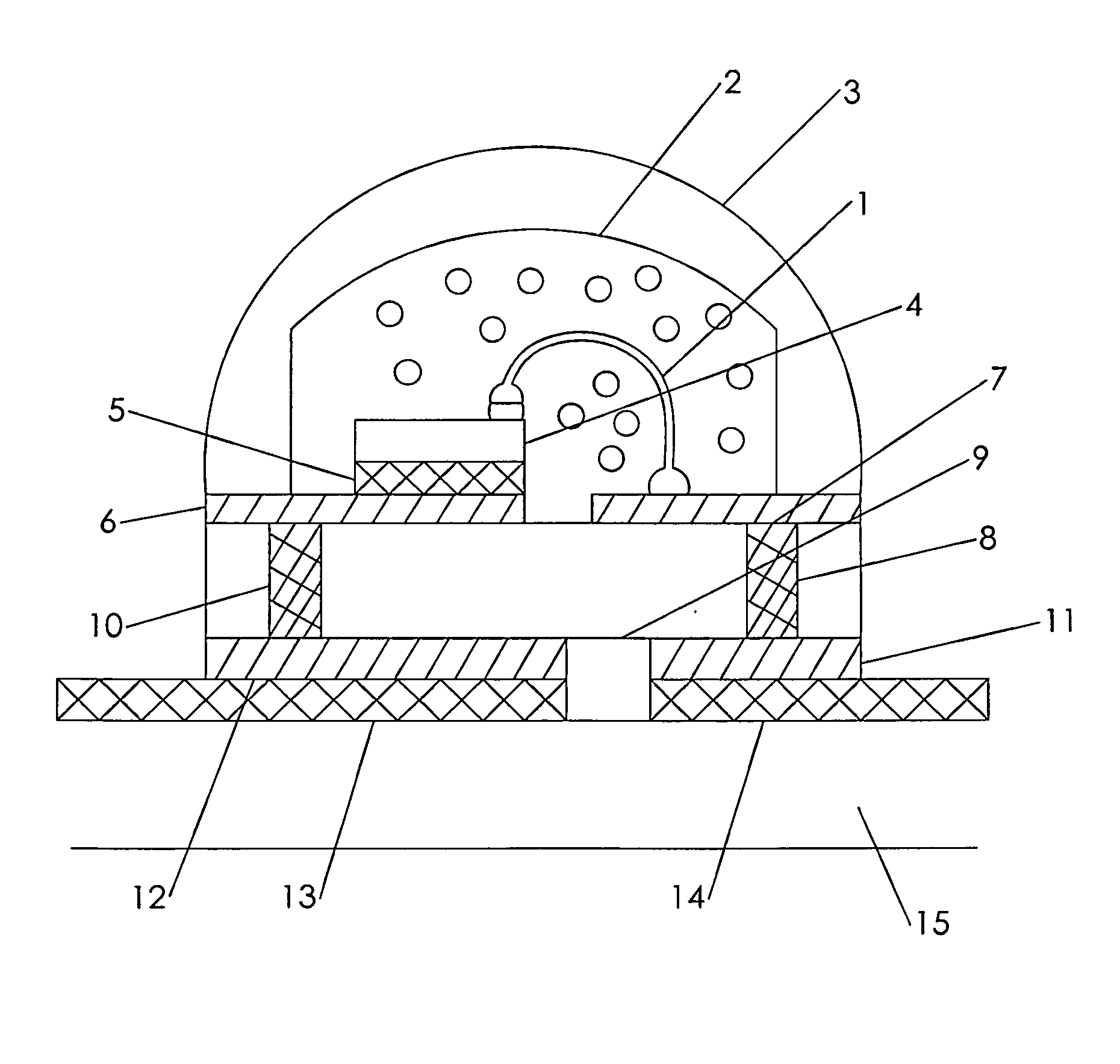
[0024]FIG. 1 illustrates a standard prior art light emitting diode (LED) package. A package is defined as containing at least one LED and at least one layer of electrical and thermal interconnect means. As an example, a blue or UV LED 4 is connected by one or more wirebonds 1 to package contact 7. In a vertical LED, the second contact is on the backside of the LED 4 with a eutectic solder layer 5 which attaches to a second package contact 6. Typically a dielectric layer 9 has internal holes (vias) 8 and 10 to the external package contacts 12 and 11. A wavelength conversion layer 2 is typically an epoxy or silicone matrix with phosphor powders dispersed within the organic matrix. This wavelength conversion layer is then bonded to a lens 3 which increases the optical extraction from the system and changes the far field optical distribution by increasing the solid angle of light which can be extracted from the LED 4 and the wavelength conversion layer 2. The external package contacts 1...


PUM


Abstract

Rapid manufacturing processes and designs based on solid luminescent elements form solid state light sources. Direct attach, as well as other LED types, are embedded or affixed to the solid luminescent elements to form low cost solid state light sources.

Description

REFERENCE TO PRIOR APPLICATION[0001]This application claims the benefit of U.S. Provisional Patent Application Ser. No. 61 / 632,165, which was filed on Jan. 18, 2012, and U.S. Provisional Patent Application Ser. No. 61 / 634,485, which was filed on Feb. 28, 2012, both of which are herein incorporated by reference.BACKGROUND OF THE INVENTION[0002]Historically, lighting has been based on self cooling inorganic designs formed using high temperature processes. This is mainly driven by the temperatures generated, the need for a controlled atmosphere envelope, and the need for environmental stability both to the light generated and the surrounding ambient environment (rain, snow, solar, dust, etc.). While LED solid state lighting sources do not typically require a controlled atmosphere envelope, the other issues remain. The need therefore exists for low cost articles and methods associated with inorganic materials for LED solid state lighting. This is especially true for luminescent material...

Claims


Application Information

Patent Timeline
Patent Type & Authority Applications(United States)
IPC IPC(8): H01L33/00H01L33/62H01L33/50
CPCH01L33/005H01L33/62H01L33/50H01L2224/32225H01L2224/48091H01L2224/48227H01L2224/48464H01L2224/73265H01L33/501H01L33/641H01L2933/0066H01L2924/181H01L2924/00014H01L2924/00H01L2924/00012
Inventor ZIMMERMAN, SCOTT M.LIVESAY, WILLIAM R.ROSS, RICHARD L.DEANDA, EDUARDOLIVESAY, CHAD R.LIVESAY, DANIEL B.
Owner GOLDENEYE
Why Eureka
Try Eureka