Self-forming embedded diffusion barriers

Active Publication Date: 2014-10-09
TESSERA LLC
View PDF8 Cites 35 Cited by
  • Summary
  • Abstract
  • Description
  • Claims
  • Application Information

AI Technical Summary

Benefits of technology

[0008]An advantage of an embodiment of the present invention is that the seed material can be deposited on top of porous low-k materials in conformal and continuous layers.
[0009]A further advantage of an embodiment of the present invention is that the seed material limits diffusion of the bulk interconnect conductor so that the barrier-forming material may form a metal oxide embedded diffusion barrier prior to the bulk interconnect conductor reaching the dielectric.
[0010]A further advantage of an embodiment of the present invention is that the seed material cre

Problems solved by technology

However, as the dimensions of microelectronic devices continue to shrink, smaller interconnect structures are also required.
As the interconnect structures shrink, the thickness of the liner becomes increasingly problematic, as it takes up a proportionally greater volume of the trench.
Because the volume

Method used


Image

  • Self-forming embedded diffusion barriers
  • Self-forming embedded diffusion barriers
  • Self-forming embedded diffusion barriers

Examples


Embodiment Construction

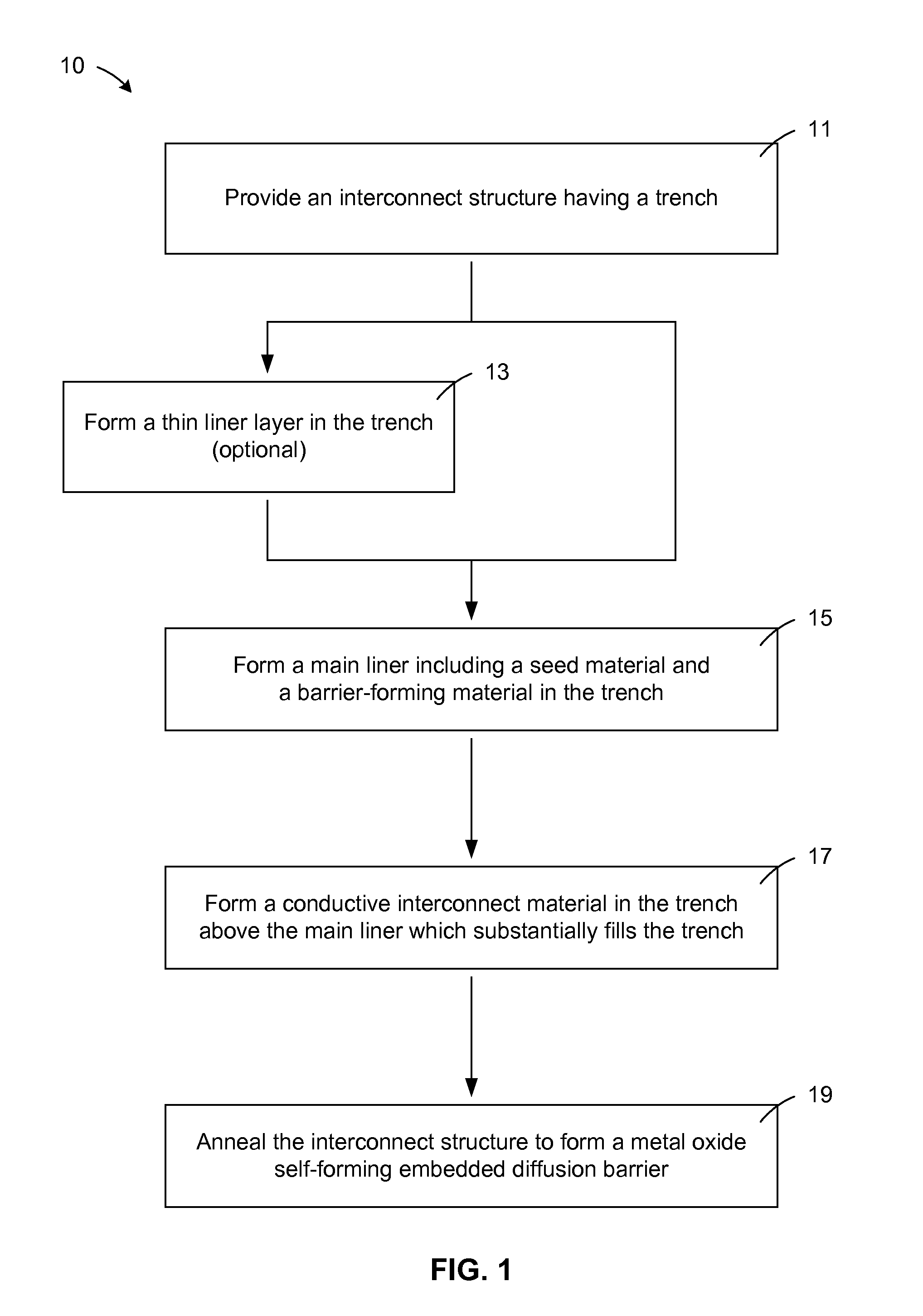
[0028]Exemplary embodiments will now be described more fully herein with reference to the accompanying drawings, in which exemplary embodiments are shown. This disclosure may, however, be embodied in many different forms and should not be construed as limited to the exemplary embodiments set forth herein. Rather, these exemplary embodiments are provided so that this disclosure will be thorough and complete and will fully convey the scope of this disclosure to those skilled in the art. In the description, details of well-known features and techniques may be omitted to avoid unnecessarily obscuring the presented embodiments.

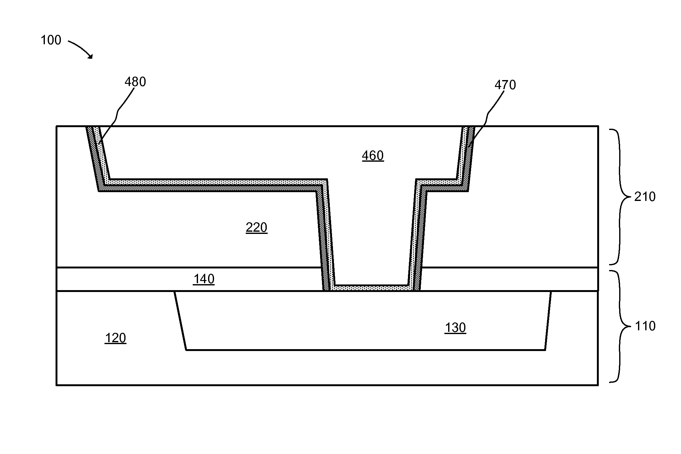
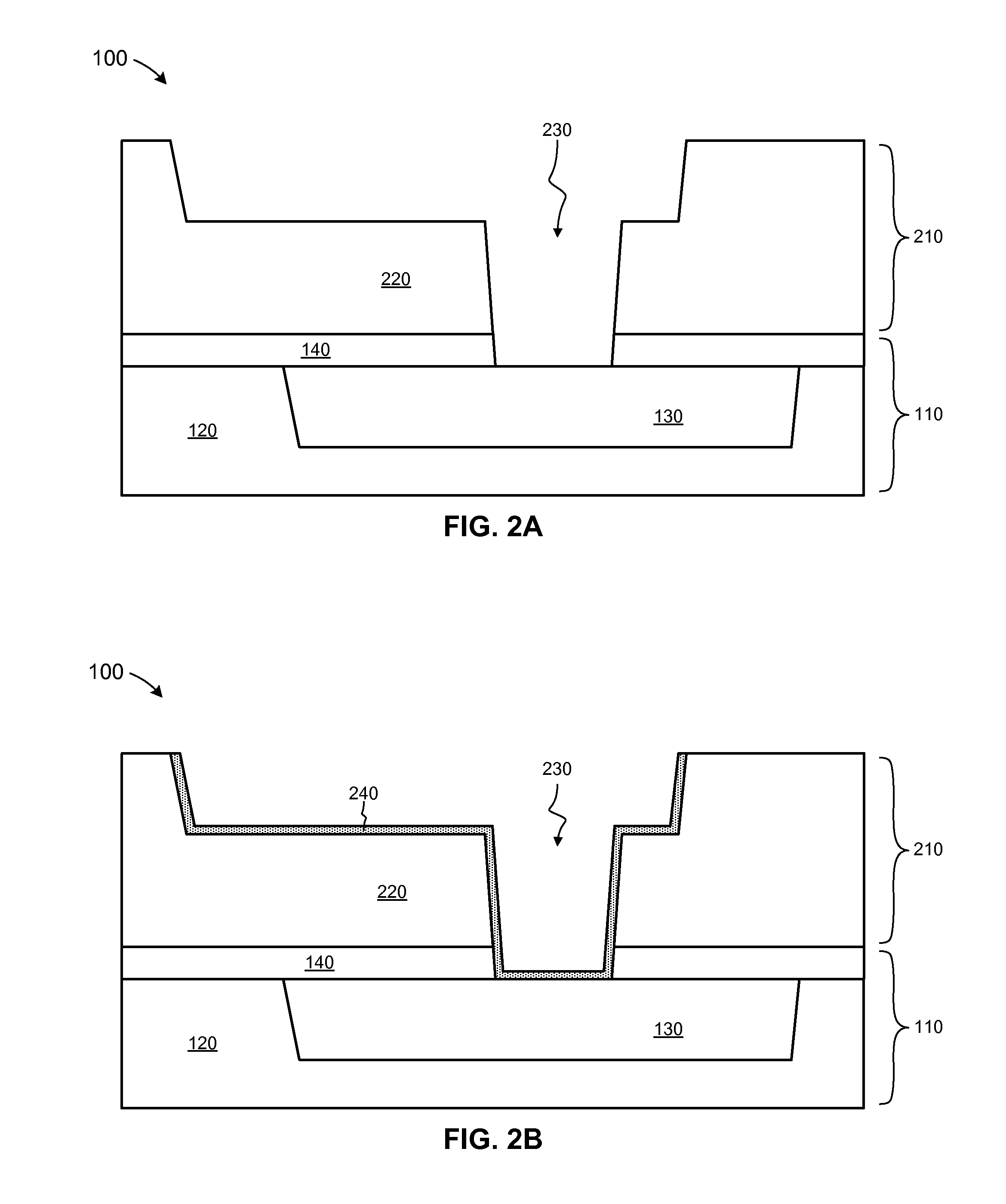
[0029]Embodiments of the invention generally relate to methods of forming an embedded diffusion barrier and a metal liner adjacent to the metal structures of interconnect levels by depositing a seed material and a barrier-forming material adjacent to the boundary of a metal structure of a back-end-of-the-line (BEOL) interconnect level. By then annealing the BEOL in...


PUM


Abstract

Interconnect structures containing metal oxide embedded diffusion barriers and methods of forming the same. Interconnect structures may include an Mx level including an Mx metal in an Mx dielectric, an Mx+1 level above the Mx level including an Mx+1 metal in an Mx+1 dielectric, an embedded diffusion barrier adjacent to the Mx+1 dielectric; and a seed alloy region adjacent to the Mx+1 metal separating the Mx metal from the Mx+1 metal. The embedded diffusion barrier may include a barrier-forming material such as manganese, aluminum, titanium, or some combination thereof. The seed alloy region may include a seed material such as cobalt, ruthenium, or some combination thereof.

Description

BACKGROUND[0001]The present invention generally relates to metal interconnect structures, and particularly to self-forming diffusion barriers.[0002]Metal interconnect structures are the primary means of connecting microelectronic devices. Such interconnect structures typically take the shape of wires, trenches, or vias formed in dielectric layers above the microelectronic devices and may typically be formed by depositing a dielectric layer, etching a trench in the dielectric layer and filling the trench with metal. To prevent electromigration of the metal within the trench and to prevent material from the metal and the dielectric from diffusing into each other, a liner may be deposited into the trench prior to filling the trench with metal. Typically, this liner consists of a layer of tantalum, tantalum nitride, or both; though other liner materials are known in the art.[0003]However, as the dimensions of microelectronic devices continue to shrink, smaller interconnect structures ar...

Claims


Application Information

Patent Timeline
IPC IPC(8): H01L21/768H01L23/532
CPCH01L21/76846H01L23/53266H01L23/53223H01L23/53209H01L23/53233H01L23/53238H01L23/53295H01L2924/0002H01L21/76831H01L21/76843H01L21/76855H01L21/76858H01L21/76867H01L21/76871H01L2924/00H01L23/528
Inventor CABRAL, JR., CYRILEDELSTEIN, DANIEL C.LI, JUNTAONOGAMI, TAKESHI
Owner TESSERA LLC
Why Eureka
Try Eureka