Power transistor gate driver

Active Publication Date: 2014-10-09
INFINEON TECH AUSTRIA AG
View PDF1 Cites 73 Cited by
  • Summary
  • Abstract
  • Description
  • Claims
  • Application Information

AI Technical Summary

Benefits of technology

[0020]The load driving assembly may be connected directly to a loudspeaker load coupled to the output terminal. The load driving assembly may for example comprise between 2 and 8 cascaded power transistors each having its drain and gate terminals coupled to a separate gate driver. According to a preferred embodiment of the load driving assembly, the second voltage supplies of the plurality of gate drivers are electrically connected to a common charge pump capacitor of the second voltage supply. This embodiment allows the plurality of second charging paths to receive their respective charging currents from a single shared high voltage supply requiring only a single capacitor. Consequently, since a typical load driving assembly may comprise more than 4 cascaded power transistor such as 6, 8 or even more, the ability to share the second voltage from a single capacitor based high voltage supply reduces the need for bootstrap capacitor to drive the gate terminals of the power transistors. So despite the common charge pump capacitor may have a considerable capacitance value such as between 10 nF and 100 nF, which requires it to be an external component to the load driving assembly, only a single capacitor component is required.
[0021]The present load driving assembly is particularly useful for application in multi-level PWM or PDM output or power stages because of their utilization of multiple stacked or cascaded power transistors. The load driving assembly may be adapted to operate at a DC voltage difference between 5 Volt and 120 Volt between the first and second DC supply voltages. According to one embodiment of the load driving assembly, adapted for use as a multi-level PWM power stage, a DC voltage source is configured to set a predetermined DC voltage difference betwe

Problems solved by technology

At that condition, the first charging path is unable of supplying further chargin

Method used


Image

  • Power transistor gate driver
  • Power transistor gate driver
  • Power transistor gate driver

Examples


Embodiment Construction

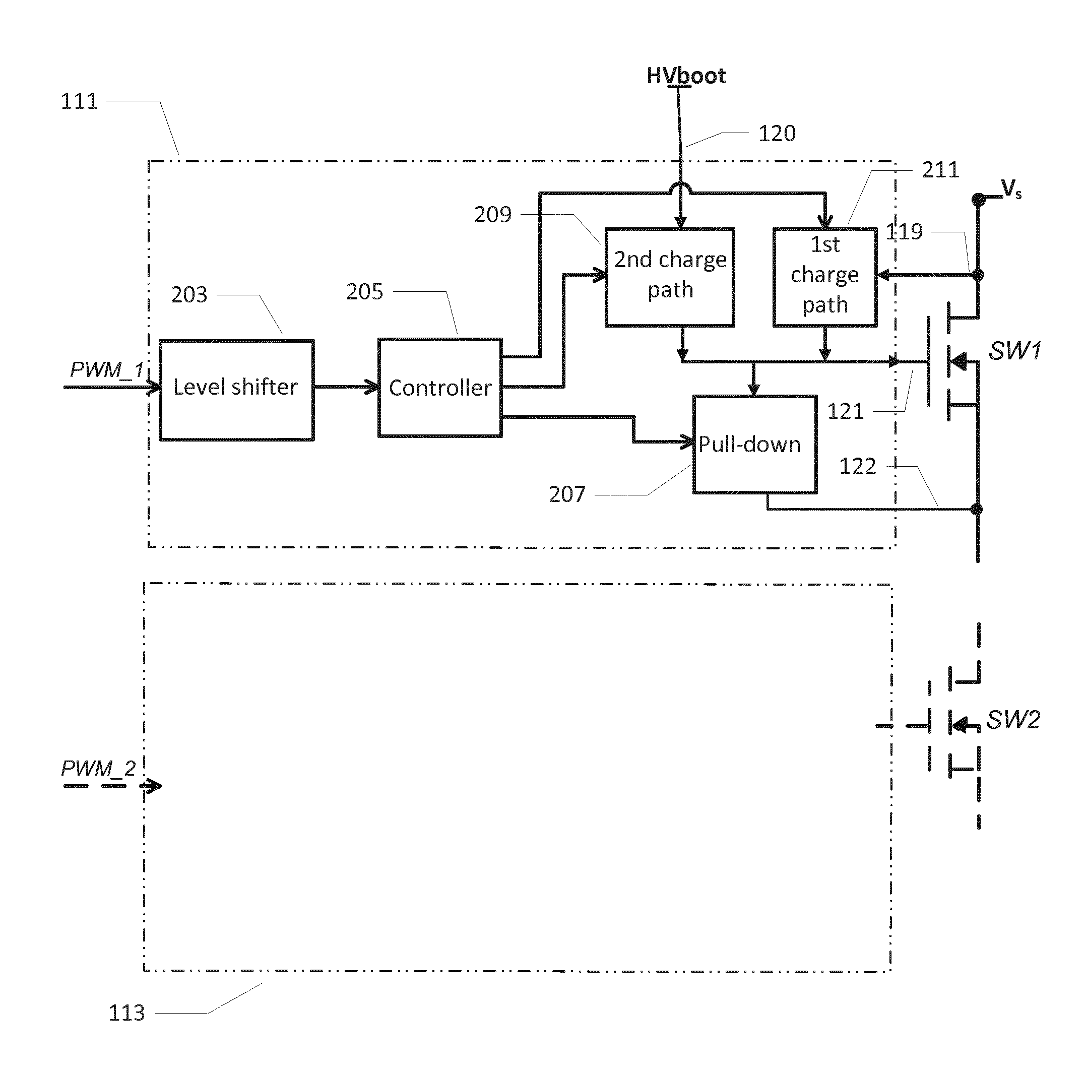
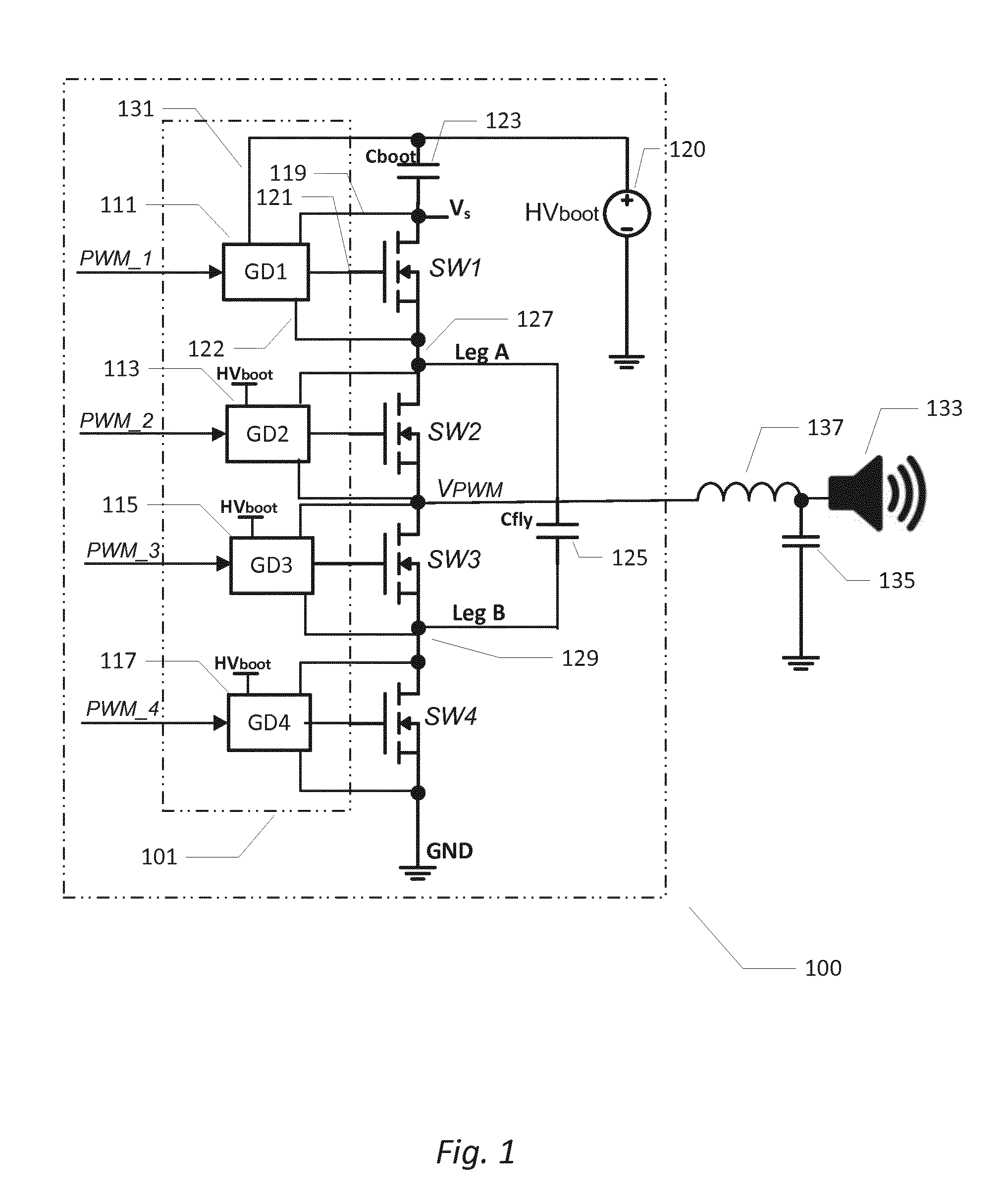
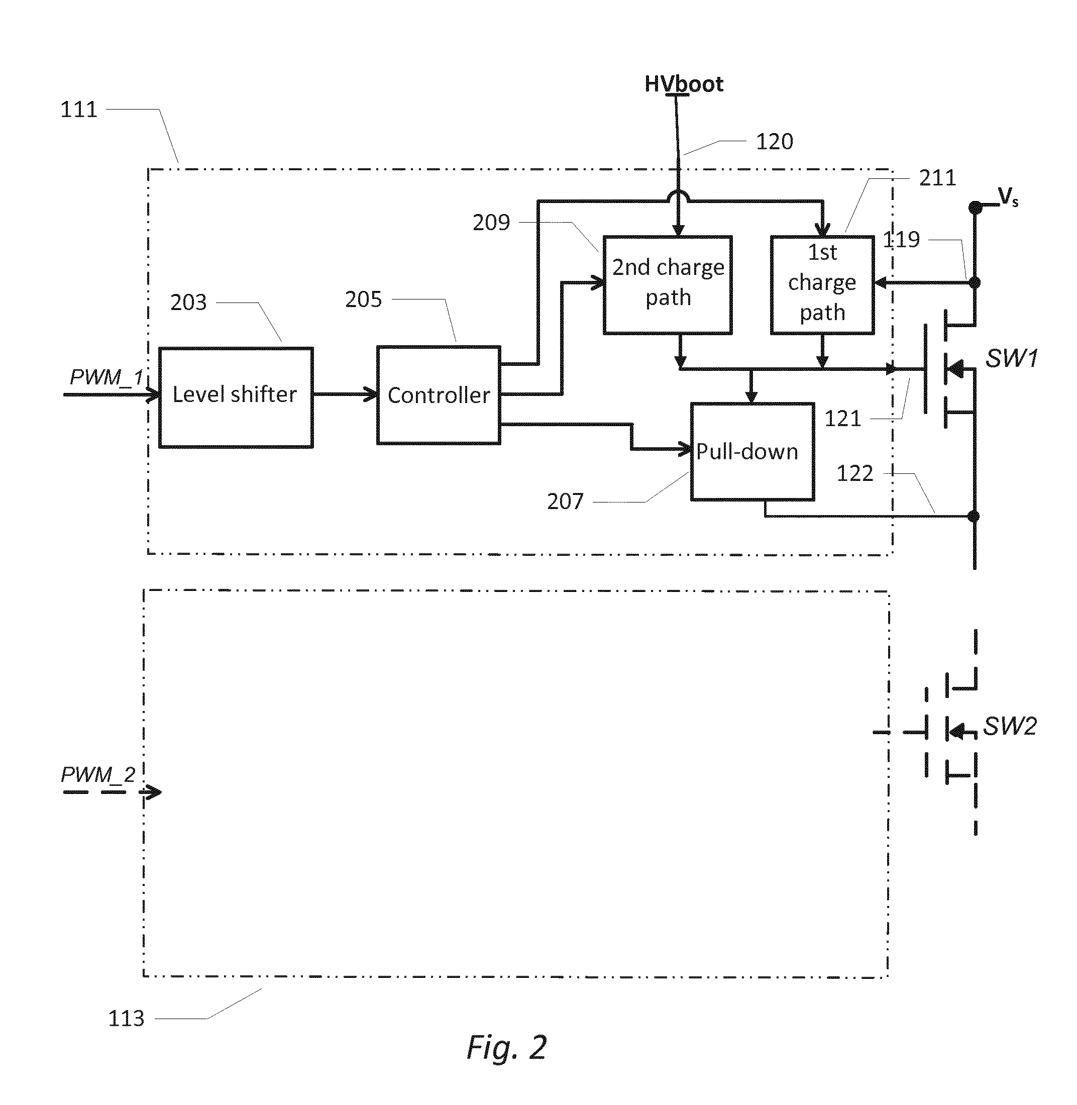
[0029]FIG. 1 illustrates schematically a load driving assembly 100 connected to a loudspeaker load 133. The load driving assembly 100 comprises a gate driving circuit 101 comprising four individual gate drivers 111, 113, 115, 117 in accordance with a preferred embodiment of the present invention. Each of the gate drivers has an output terminal electrically connected to a gate terminal of one of NMOS transistors SW1, SW2, SW3, SW4. The NMOS transistors SW1, SW2, SW3, SW4 are coupled in cascade between a first or positive DC supply voltage VS and a second DC supply voltage in form of ground, GND. The cascaded NMOS transistors SW1, SW2, SW3, SW4 form a load driver for the loudspeaker load 133 coupled to an output terminal VPWM of the load driver through a load inductor 137 and a load capacitor 135. The combined operation of the load capacitor and load inductor 135, 137, respectively, is to provide lowpass filtering of a multi-level pulse width modulated output signal waveform provided ...


PUM


Abstract

The present invention relates to a gate driver for a power transistor comprising a first charging path operatively connected between a first voltage supply and a gate terminal of the power transistor for charging the gate terminal to a first gate voltage. A second charging path is connectable between the gate terminal of the power transistor and a second supply voltage to charge the gate terminal from the first gate voltage to a second gate voltage larger or higher than the first gate voltage. A voltage of the second voltage supply is higher than a voltage of the first voltage supply.

Description

[0001]The present invention relates to a gate driver for a power transistor comprising a first charging path operatively connected between a first voltage supply and a gate terminal of the power transistor for charging the gate terminal to a first gate voltage. A second charging path is connectable between the gate terminal of the power transistor and a second supply voltage to charge the gate terminal from the first gate voltage to a second gate voltage larger or higher than the first gate voltage. A voltage of the second voltage supply is higher than a voltage of the first voltage supply. Another aspect of the invention relates to a load driving assembly comprising a plurality of gate drivers electrically coupled to respective ones of a plurality of power transistors. The load driving assembly may be utilized in various power amplification applications such as class D audio amplifiers.BACKGROUND OF THE INVENTION[0002]Gate drivers for power transistors of a power or output stage of...

Claims


Application Information

Patent Timeline
IPC IPC(8): H03K17/687H03F3/217
CPCH03F3/2171H03K17/687H02M1/08H03F3/2173H03K17/063H03K17/6871H02M7/4837
Inventor HOYERBY, MIKKELJAKOBSEN, JORGEN KRAGH
Owner INFINEON TECH AUSTRIA AG
Why Eureka
Try Eureka