Inspection apparatus

a technology of inspection apparatus and test tube, which is applied in the direction of liquid/fluent solid measurement, machines/engines, instruments, etc., can solve the problems of difficult to reduce the cost of the apparatus, difficult to completely prevent foreign matter (particles) from adhering to the sample surface, and high cost of the drive motor made of non-magnetic material

Active Publication Date: 2014-10-23
EBARA CORP
View PDF2 Cites 25 Cited by
  • Summary
  • Abstract
  • Description
  • Claims
  • Application Information

AI Technical Summary

Problems solved by technology

However, the drive motor made of nonmagnetic material is expensive (e.g., more expensive than a linear motor), which causes a problem in that it is difficult to reduce the cost of the apparatus.
Also in the conventional inspection apparatus, it is difficult to completely prevent foreign matters (particles) from adhering to a sample surface.

Method used


Image

  • Inspection apparatus
  • Inspection apparatus
  • Inspection apparatus

Examples


embodiment 1

Semiconductor Inspection Apparatus Including Double Pipe Structure Lens Tube

[0174]As described above, the electronic optical device 70 including the primary optical system 2100, which is described as the second embodiment of the primary optical system according to the invention of this application, is different in setting of voltages applied to the respective configurational components from a typical electron gun. That is, reference potential V2 is used as the high voltage (e.g., +40000 V). First, the semiconductor inspection apparatus 1 including the electronic optical device 70 according to the invention of this application has a double pipe structure.

[0175]Description will be made with reference to FIG. 10. FIG. 10 is a diagram schematically showing the double pipe structure of the semiconductor inspection apparatus according to one embodiment of the present invention. In FIG. 10, the first pipe and the second pipe are emphasized. The sections of the actual first pipe and second ...

first embodiment

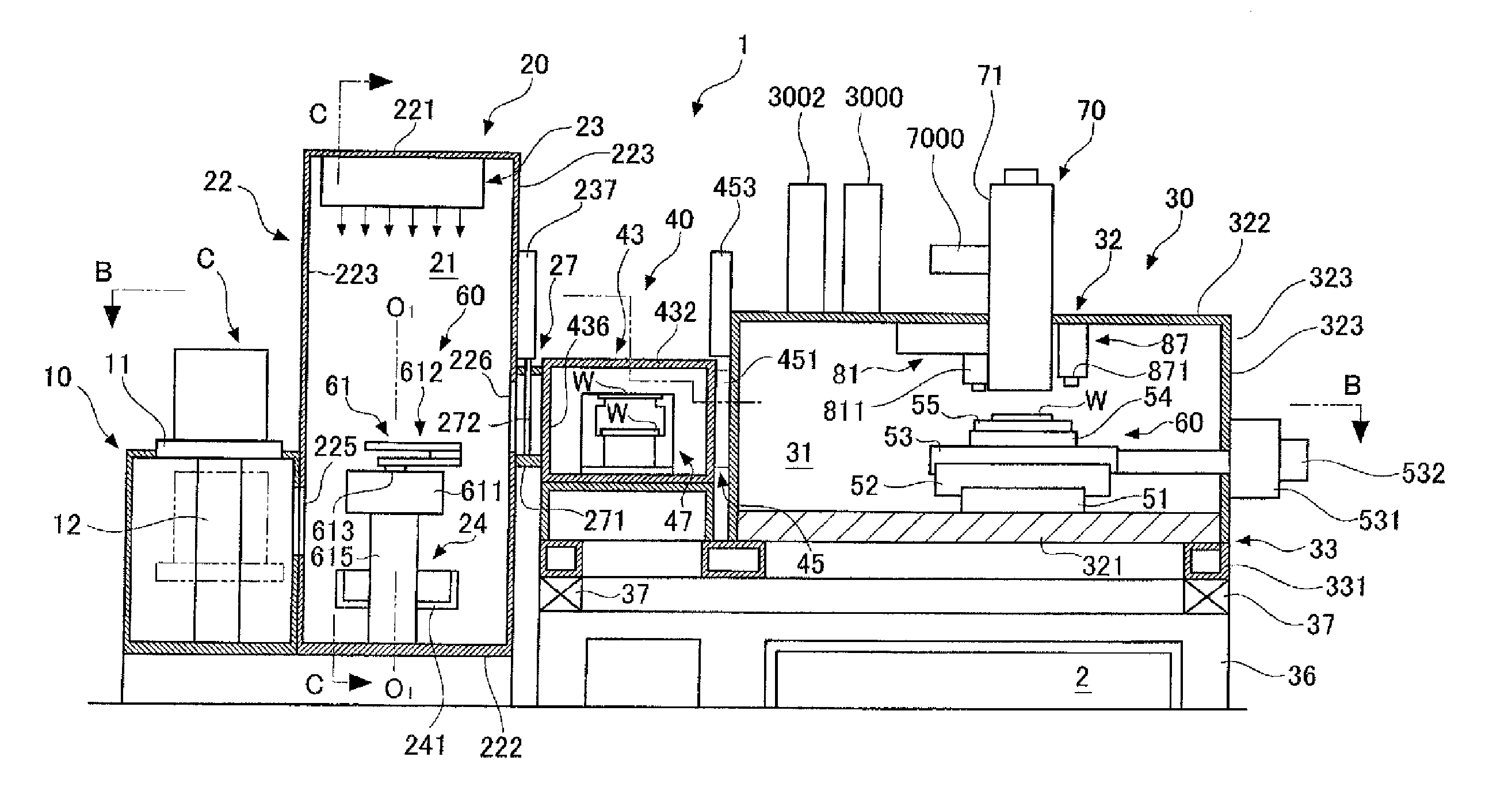
[0326]A configuration of an inspection apparatus of a first embodiment of the present invention is described with reference to FIG. 33. FIG. 33 is a diagram illustrating a main part of the inspection apparatus of this embodiment. As shown in FIG. 33, the inspection apparatus 10-2 of this embodiment includes a cover member 28-2 that blocks a gap between a gap control plate 24-2 and a condenser lens 26-2 (also see FIG. 34). The gap control plate 24-2 is arranged above the stage 14-2 so as to cover the surface of the sample 16-2 arranged on the stage 14-2. A through hole 24a-2 allowing an electron beam to pass therethrough is provided at the center (inside) of the gap control plate 24-2. A condenser lens 26-2 in a secondary system lens is arranged in the through hole 24a-2. The material of the cover member 28-2 is an insulator (e.g., a ceramic or Teflon (registered trademark)).

[0327]As shown in FIG. 33, in view of the direction perpendicular to the gap control plate 24-2 (sight directi...

second embodiment

[0332]Next, an inspection apparatus of a second embodiment of this the present invention is described. Here, the difference of the inspection apparatus of the second embodiment from the apparatus of the first embodiment is mainly described. Unless otherwise noted, the configuration and operation of this embodiment is analogous to those of the first embodiment.

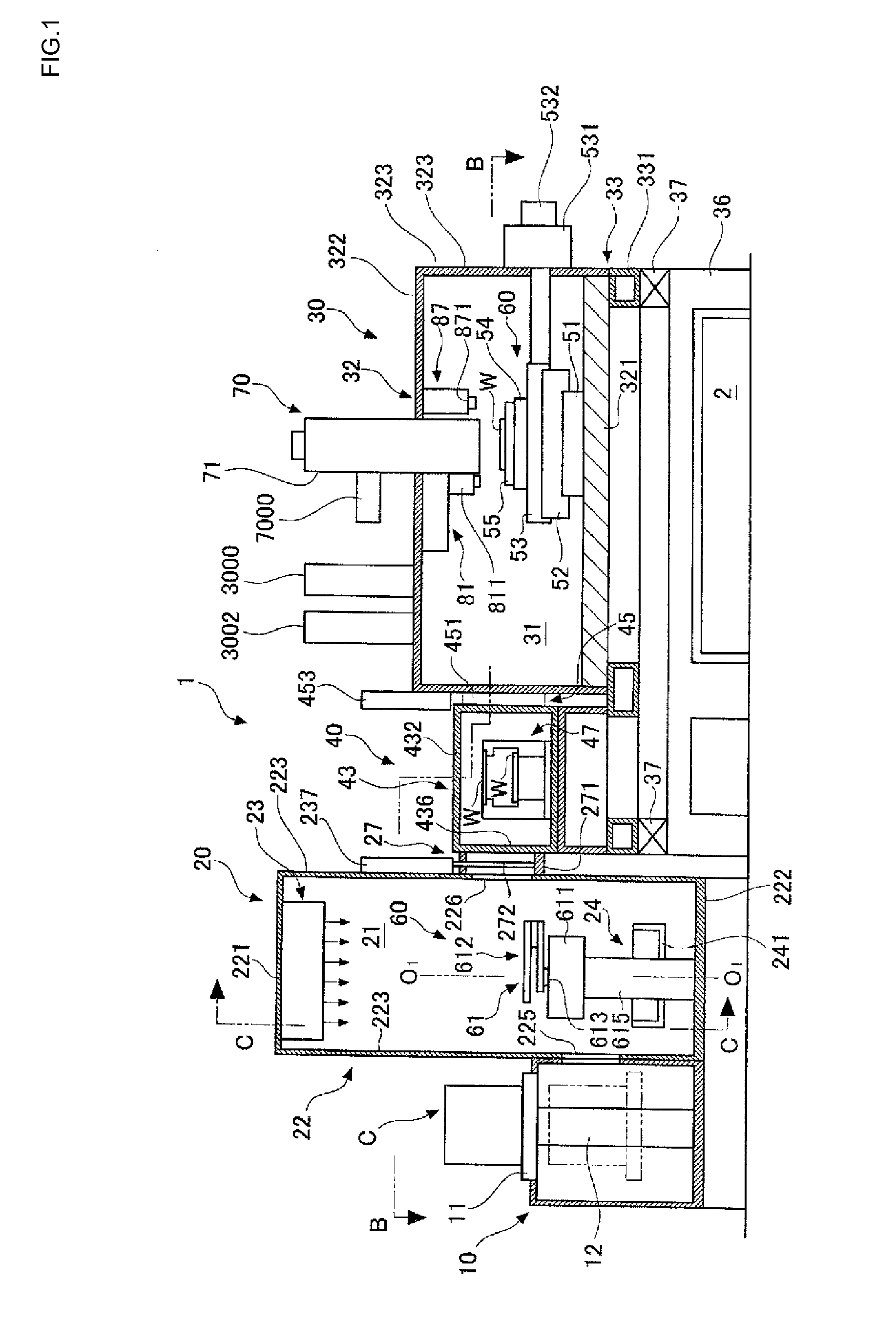
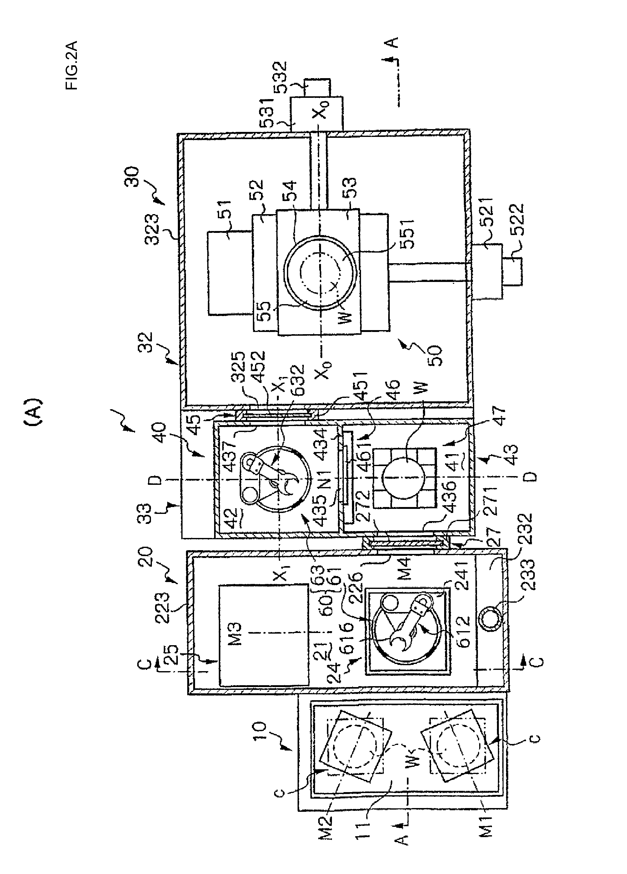
[0333]FIG. 34 is a diagram illustrating the inspection apparatus of this embodiment. As shown in FIG. 34, an inspection apparatus 10-2 of this embodiment does not include a dust collector 22-2 for reducing adhesion of foreign matters to a sample surface (also see FIG. 35). In this case, the width D of a gap between a through hole 24a-2 and a condenser lens 26-2 viewed in a direction perpendicular to a gap control plate 24-2 (sight direction) ranges from 5 to 30 mm.

[0334]According to such an inspection apparatus of a second embodiment of the present invention, the width of the gap (a gap viewed in the direction perpendicular to ...


PUM

PropertyMeasurementUnit
widthaaaaaaaaaa
sizeaaaaaaaaaa
sizeaaaaaaaaaa

Abstract

An inspection apparatus capable of facilitating reduction in cost of the apparatus is provided. The inspection apparatus includes: beam generation means for generating any of charged particles and electromagnetic waves as a beam; a primary optical system that guides the beam into an inspection object held on a movable stage in a working chamber and irradiates the inspection object with the beam; a secondary optical system that detects secondary charged particles occurring from the inspection object; and an image processing system that forms an image on the basis of the detected secondary charged particles. The inspection apparatus further includes: a linear motor that drives the movable stage; and a Helmholtz coil that causes a magnetic field for canceling a magnetic field caused by the linear motor when the movable stage is driven.

Description

BACKGROUND OF THE INVENTION[0001]1. Field of the Invention[0002]The present invention (first aspect) relates to an inspection apparatus that inspects defects of a pattern formed on a surface of an inspection object, and specifically, to an inspection apparatus that captures secondary charged particles varying properties of a surface of an inspection object, forms image data, and inspects a pattern and the like formed on the surface of the inspection object on the basis of the image data at a high throughput, and an inspection method.[0003]Furthermore, the present invention (second aspect) relates to an inspection apparatus that inspects a sample surface using an electron beam and, particularly, to an inspection apparatus that can inspect sample surfaces (front, rear and outer peripheral surfaces) at high sensitivity using an electron beam while preventing foreign matters from adhering to the sample surfaces.[0004]2. Description of the Related Art[0005](First Aspect)[0006]A conventio...

Claims


Application Information

Patent Timeline
Patent Type & Authority Applications(United States)
IPC IPC(8): G01N23/22G01N21/95H01J37/02
CPCG01N23/2204G01N21/9501H01J37/02H01J37/09H01J37/16H01J37/20H01J37/285H01J2237/022H01J2237/0264H01J2237/1501H01J2237/166H01J2237/2007H01J2237/20221H01J2237/20278H01J37/023H01J2237/20H01J2237/26
Inventor YOSHIKAWA, SHOJITSUKAMOTO, KIWAMU
Owner EBARA CORP
Why Eureka
Try Eureka