Defective p-n junction for backgated fully depleted silicon on insulator mosfet

a technology of fully depleted silicon and insulator mosfet, which is applied in the direction of semiconductor devices, basic electric elements, electrical apparatus, etc., can solve the problems of fluctuation of actual backbais, and achieve the effect of reducing leakage resistance of the p-n junction

Active Publication Date: 2014-10-23
TAIWAN SEMICON MFG CO LTD +2
View PDF4 Cites 2 Cited by
  • Summary
  • Abstract
  • Description
  • Claims
  • Application Information

AI Technical Summary

Benefits of technology

[0005]A method for semiconductor fabrication includes forming a well in a semiconductor substrate. A pocket is formed within the well, the pocket having an opposite doping polarity as the well to provide a p-n junction between the well and the pocket. Defects are created at the p-n junction such that a leakage resistance of the p-n junction is decreased.
[0006]A method for semiconductor fabrication includes forming a well in a semiconductor substrate. A pocket is formed within the well, the pocket having an opposite doping polarity as the well to provide a p-n junction between the well and the pocket, wherein the pocket is formed under an isolation layer of the semiconductor substrate. Defects are created at the p-n junction such that a leakage resistance of the p-n junction is decreased, wherein the defects are created as part of a same implantation used to form the pocket.
[0007]A semiconductor device includes a semiconductor substrate having a well formed therein. A pocket is formed within the well, the pocketing having an opposite doping polarity as the well to provide a p-n junction between the well and the pocket. Defects are created at the p-n junction such that a leakage resistance of the p-n junction is decreased.

Problems solved by technology

However, during AC operation, there is a capacitive voltage divider formed by the MOS (metal-oxide-semiconductor) capacitor associated with the BOX and the depletion capacitor associated with the p-n junction between the well and pocket such that not all of the voltage drops across the BOX, causing the actual backbais to fluctuate.

Method used


Image

  • Defective p-n junction for backgated fully depleted silicon on insulator mosfet
  • Defective p-n junction for backgated fully depleted silicon on insulator mosfet
  • Defective p-n junction for backgated fully depleted silicon on insulator mosfet

Examples


Embodiment Construction

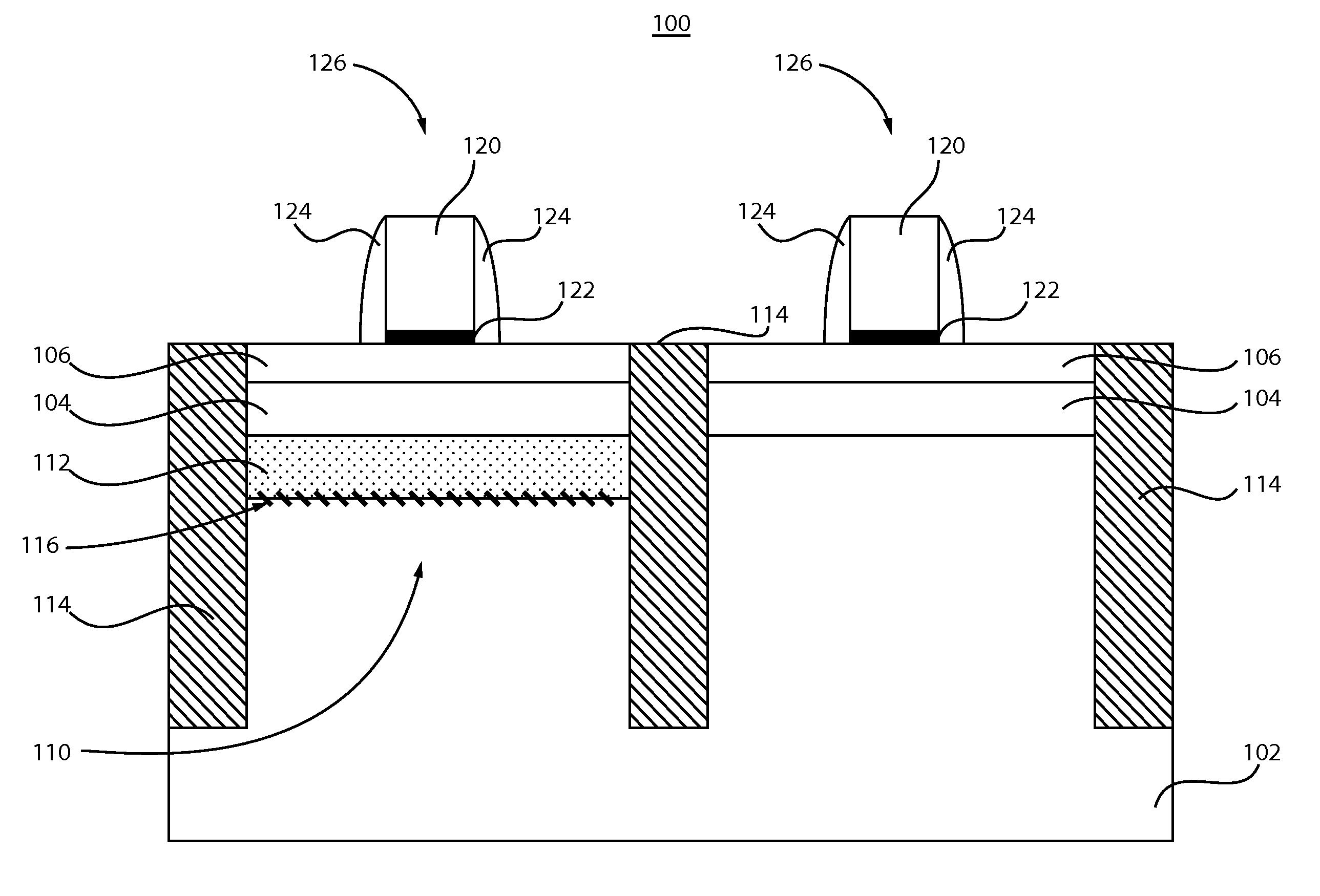
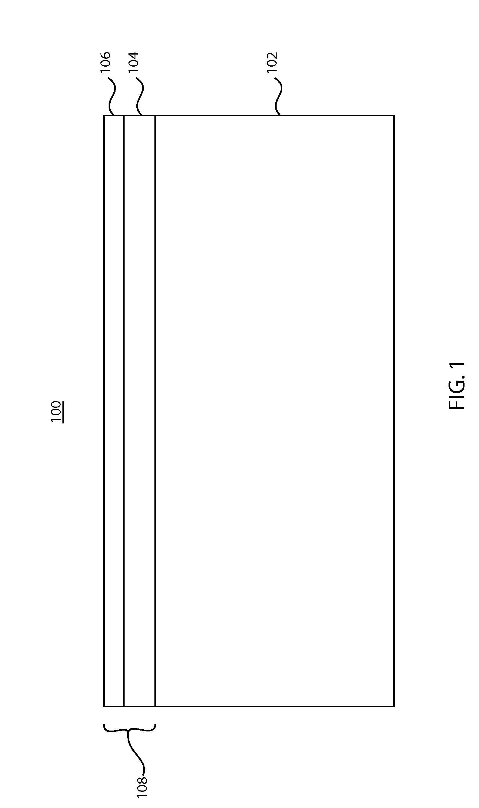
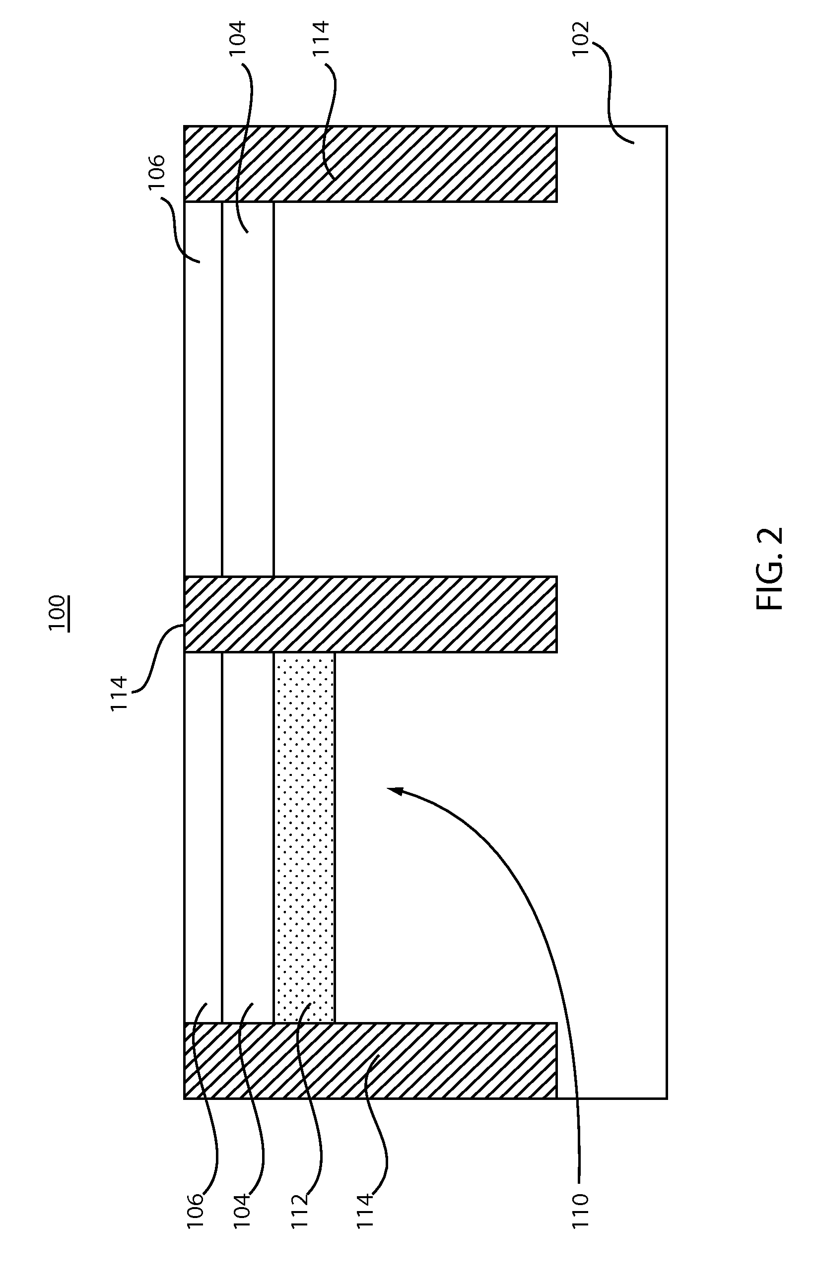
[0017]In accordance with the present principles, methods and semiconductor devices are provided for a defective p-n junction for backgated fully depleted semiconductor-on-insulator (FDSOI) MOSFETs (metal-oxide-semiconductor field-effect transistor). The FDSOI includes a well and a pocket formed within the well. Defects are formed at the interface between the well and the pocket. Preferably, the interface includes a p-n junction. The defects may include end-of-range implant defects or impurities that generate mid-gap states. In one embodiment, the defects are formed as part of a same implantation used to form the pocket. In another embodiment, the defects are formed by a separate blanket implantation.

[0018]One advantage of the present principles is that defects are formed at the interface between the pocket and the well such that the junction is leaky. During AC (alternating current) operation, most of the applied voltage drops at the buried oxide interface.

[0019]It is to be understo...


PUM

PropertyMeasurementUnit
threshold voltageaaaaaaaaaa
thicknessesaaaaaaaaaa

Abstract

Methods for semiconductor fabrication include forming a well in a semiconductor substrate. A pocket is formed within the well, the pocket having an opposite doping polarity as the well to provide a p-n junction between the well and the pocket. Defects are created at the p-n junction such that a leakage resistance of the p-n junction is decreased.

Description

BACKGROUND[0001]1. Technical Field[0002]The present invention relates to semiconductor fabrication, and more particularly to forming a defective p-n junction for backgated fully depleted silicon on insulator devices.[0003]2. Description of the Related Art[0004]In ultrathin fully depleted silicon on insulator (FDSOI) with thin buried oxide (BOX), pocket implants are placed underneath the BOX to adjust the threshold voltage Vt of the transistors. For example, with a BOX thickness of about 25 nm, changing the implant polarity shifts the threshold voltage by about 80 mV. To modulate the threshold voltage of the transistors during operation, a backgate voltage (backbias) is applied. To minimize the area penalty for connecting the backbias, it is applied to a well that is shared by several transistors. For those transistors that have a pocket implant, the backbias is applied to the BOX through a p-n junction that is located in series with the BOX. Since there is no DC current flowing thro...

Claims


Application Information

Patent Timeline
Patent Type & Authority Applications(United States)
IPC IPC(8): H01L21/761H01L29/06
CPCH01L29/0684H01L21/761H01L21/76283H01L21/84H01L29/78648H01L27/1203H01L29/66772H01L29/78612H01L21/2253H01L21/7624H01L21/76243H01L29/66477
Inventor CHENG, KANGGUODORIS, BRUCE B.GRENOUILLET, LAURENTKHAKIFIROOZ, ALILE TIEC, YANNICKLIU, QINGVINET, MAUD
Owner TAIWAN SEMICON MFG CO LTD
Why Eureka
Try Eureka