Integrated circuit package and method for manufacturing the same

a technology of integrated circuits and components, applied in the direction of electrical equipment, semiconductor devices, semiconductor/solid-state device details, etc., can solve the problems of long time-consuming and labor-intensive laser machining process for forming via holes, inability to rewire the upper integrated circuit package, and limited number of i/o terminals

Inactive Publication Date: 2014-10-23
STS SEMICON & TELECOMM
View PDF4 Cites 39 Cited by
  • Summary
  • Abstract
  • Description
  • Claims
  • Application Information

AI Technical Summary

Benefits of technology

[0016]Therefore, the present invention has been made in view of the above problems, and it is an object of the present invention to provide a stacked integrated circuit package which can substantially address various problems caused by limitations and disadvantages of the conventional technology and a method for manufacturing the same.

Problems solved by technology

However, in the case on the conventional TMV-type stacked integrated circuit package described above, laser machining process for formation of a via hole takes a long time, and the number of I / O terminals is limited.
Further, rewiring on the upper integrated circuit package is substantially impossible.
Thereby, circuit design for the conventional TMV-type stacked integrated circuit package is difficult.

Method used


Image

  • Integrated circuit package and method for manufacturing the same
  • Integrated circuit package and method for manufacturing the same
  • Integrated circuit package and method for manufacturing the same

Examples


Embodiment Construction

[0034]Reference will now be made in detail to the embodiments of the present invention, examples of which are illustrated in the accompanying drawings.

[0035]In describing the present invention, a detailed description of well-known functions and constituents will be omitted if such description might unnecessarily obscure the main points of the present invention. In addition, terms which will be used below are defined in consideration of the functions of the present invention. The definitions of the terms may vary depending on intention of a user or a precedent case. Therefore, the terms should be defined based on the entire specification.

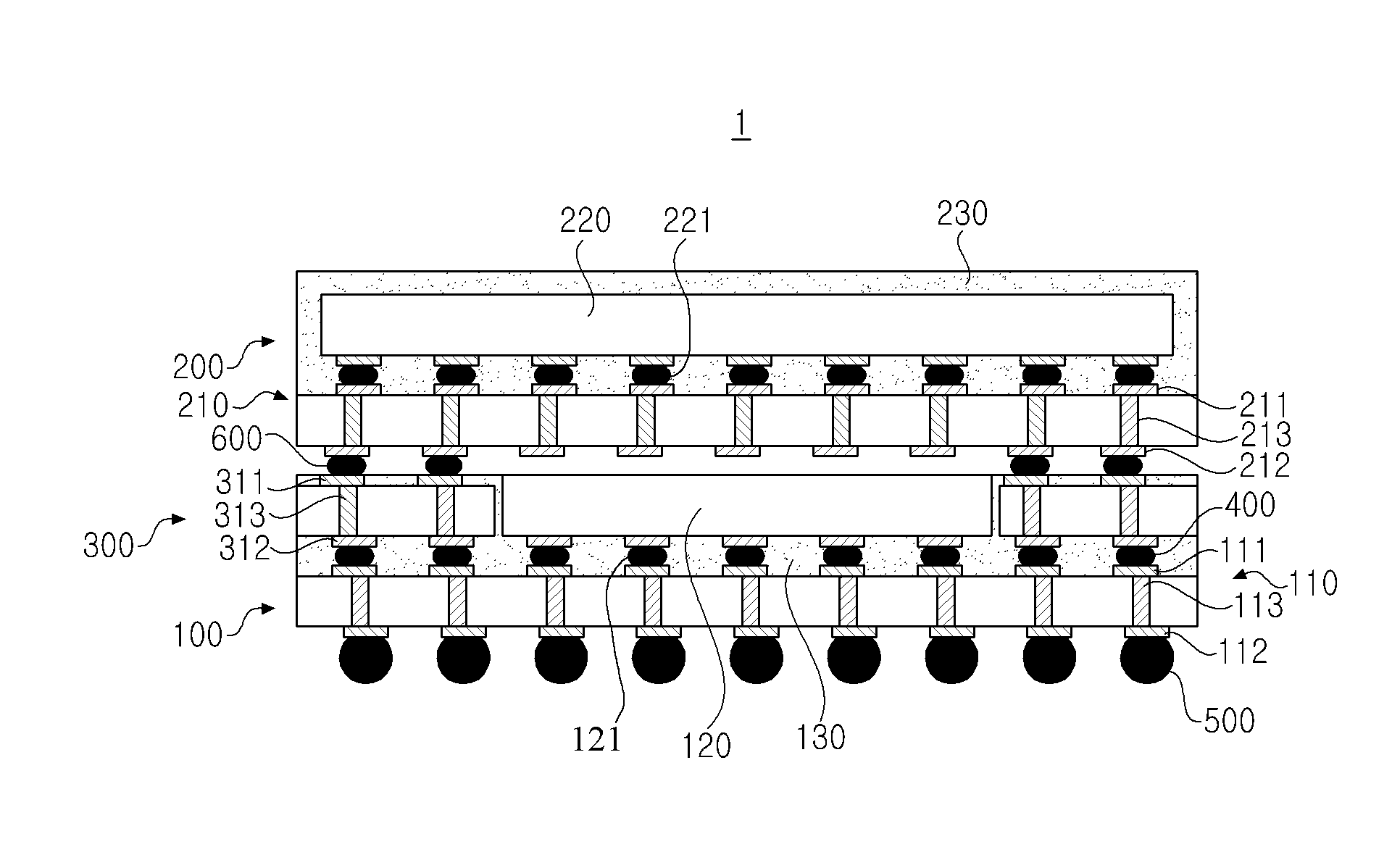
[0036]FIG. 2 is a cross-sectional view showing the structure of a stacked integrated circuit package according to an exemplary embodiment of the present invention.

[0037]FIG. 3 is a plan view showing the configuration of an interposer according to an embodiment of the present invention.

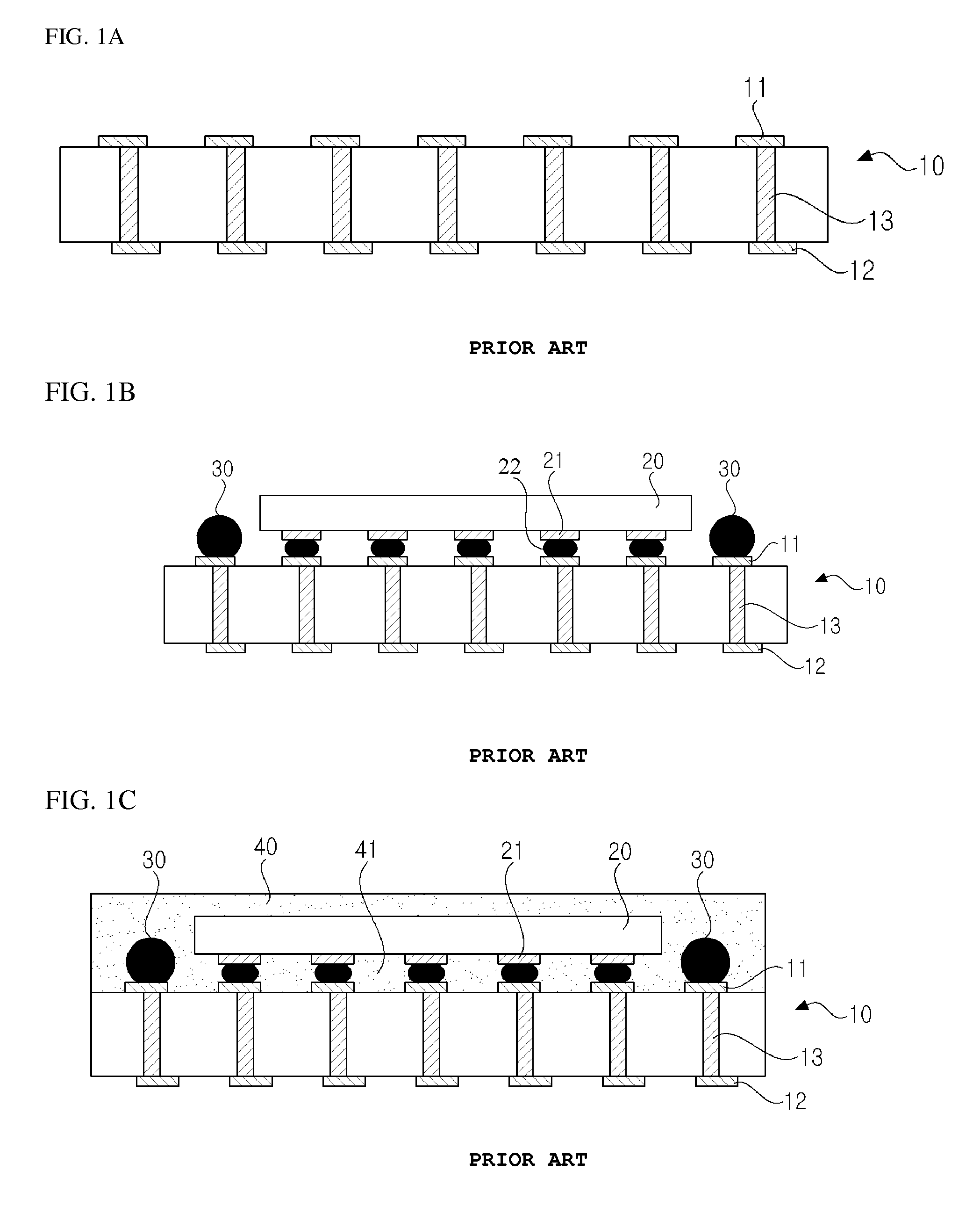
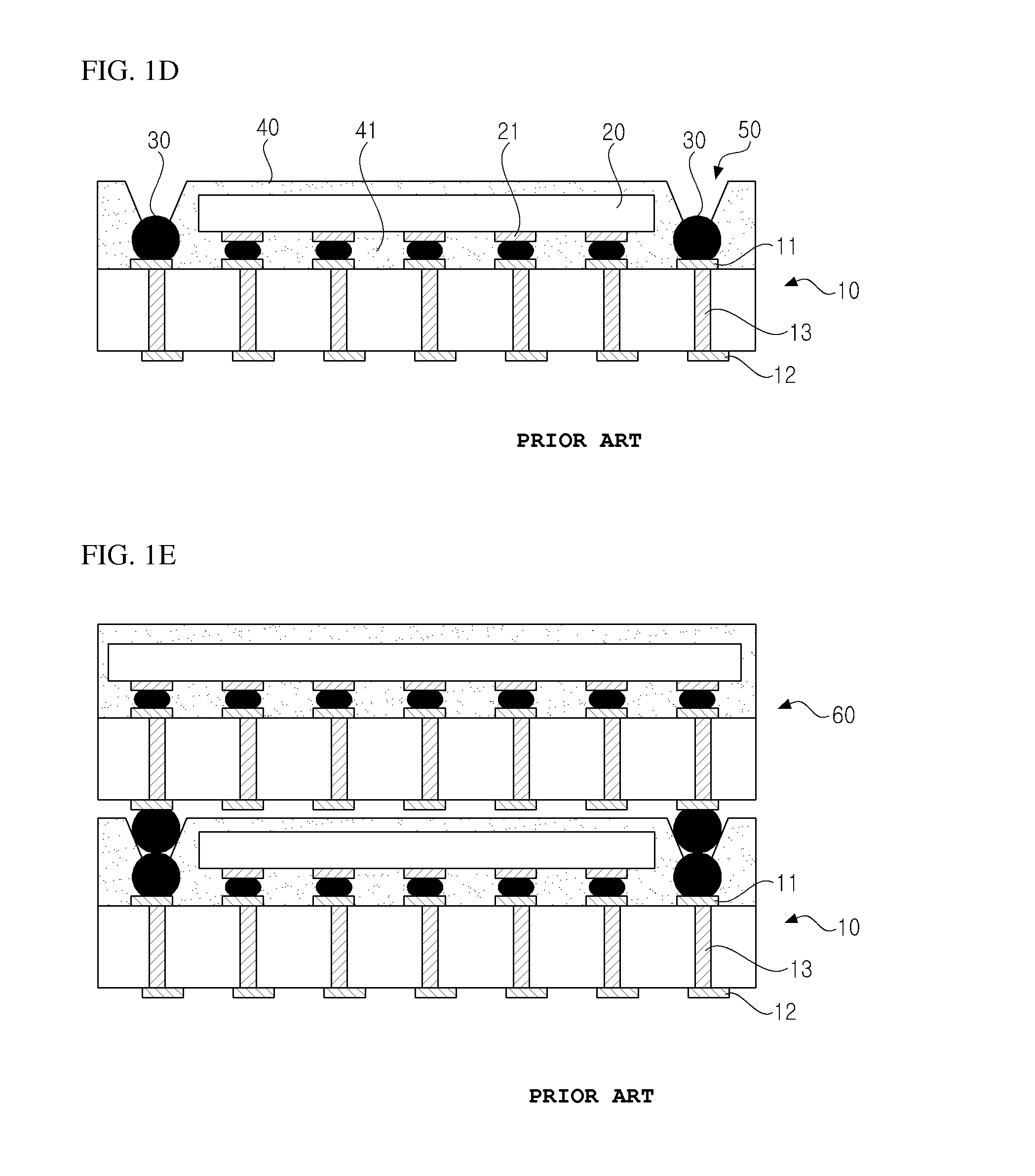
[0038]FIGS. 4A to 4F are cross-sectional views illustrating the pr...


PUM


Abstract

A stacked integrated circuit package and a method for manufacturing the same are provided.
The stacked integrated circuit package includes a first integrated circuit package comprising a first substrate, a first semiconductor chip, and a first molding portion, an interposer mounted on the first substrate to be electrically connected to the circuit pattern of the first substrate by a first solder bump, the interposer being provided with an opening to accommodate the first semiconductor chip, and a second integrated circuit package stacked on the first integrated circuit package and the interposer and electrically connected to the interposer by a second solder bump, the second integrated circuit package comprising a second substrate, a second semiconductor chip, and a second molding portion.

Description

BACKGROUND OF THE INVENTION[0001]1. Field of the Invention[0002]The present invention relates to an integrated circuit package, and more particularly to a stacked integrated circuit package having a package-on-package structure and a method for manufacturing the same.[0003]2. Description of the Related Art[0004]In the semiconductor industry, a product having light weight, compact size, multi-functionality and high performance is generally demanded. One technology necessary to meet such demand is integrated circuit packaging.[0005]Integrated circuit packaging is a technology of forming input / output signal terminals to a main board using a lead frame or a printed circuit board and molding the terminals with a encapsulant to protect a semiconductor chip such as a single device and an integrated circuit, formed by stacking electric circuits and wires, from various external environmental factors such as dust, moisture, and electric and mechanical loads and to optimize or maximize electri...

Claims


Application Information

Patent Timeline
Patent Type & Authority Applications(United States)
IPC IPC(8): H01L25/065H01L25/00
CPCH01L25/50H01L25/0657H01L2924/15311H01L25/105H01L2225/1023H01L2225/1041H01L2225/1058H01L24/13H01L24/16H01L24/48H01L24/81H01L24/85H01L2224/131H01L2224/16227H01L2224/48227H01L2224/81801H01L2924/00014H01L23/3128H01L2224/16225H01L2924/12042H01L23/49811H01L23/49827H01L23/49833H01L23/49838H01L2924/3511H01L2924/181H01L2924/014H01L2224/45099H01L2924/00H01L2924/00012
Inventor CHOI, DAESIKOH, SEUNG HOON
Owner STS SEMICON & TELECOMM
Why Eureka
Try Eureka