Methods For Thick Films Thermoelectric Device Fabrication

a thermoelectric device and thick film technology, applied in the manufacture/treatment of thermoelectric devices, superimposed coating processes, coatings, etc., can solve the problems of no progress in developing a process by which the semiconductor remains pure, and achieves high free volume, sufficient structural integrity, and reduced reactions

Active Publication Date: 2014-10-23
ATS IP LLC
View PDF6 Cites 7 Cited by
  • Summary
  • Abstract
  • Description
  • Claims
  • Application Information

AI Technical Summary

Benefits of technology

[0030]An object of the present invention is to provide a method by which to fabricate thick films in a manner that reduces reactions between the thick film and the substrate on which it is deposited by producing a layer with a high free volume after vehicle volatilization. The layer is heated and during the volatilization process becomes sintered such that it acquires sufficient structural integrity for further processing. The thick film can be densified by pressing to obtain desired material properties such as electrical and thermal conductivity, thereby providing a direct bond process of a thick film to a substrate with sufficient chemical and / or mechanical adhesion and with limited reaction at the thick film-metal interface.

Problems solved by technology

Research in thick film methods have been reported, though there has been no progress in developing a process by which the semiconductor remains pure or is directly bonded to the metal substrate.

Method used


Image

  • Methods For Thick Films Thermoelectric Device Fabrication
  • Methods For Thick Films Thermoelectric Device Fabrication
  • Methods For Thick Films Thermoelectric Device Fabrication

Examples


Embodiment Construction

[0040]The following description presents various inventions, and example embodiments thereof. The various inventions and examples described can be useful alone or in combinations.

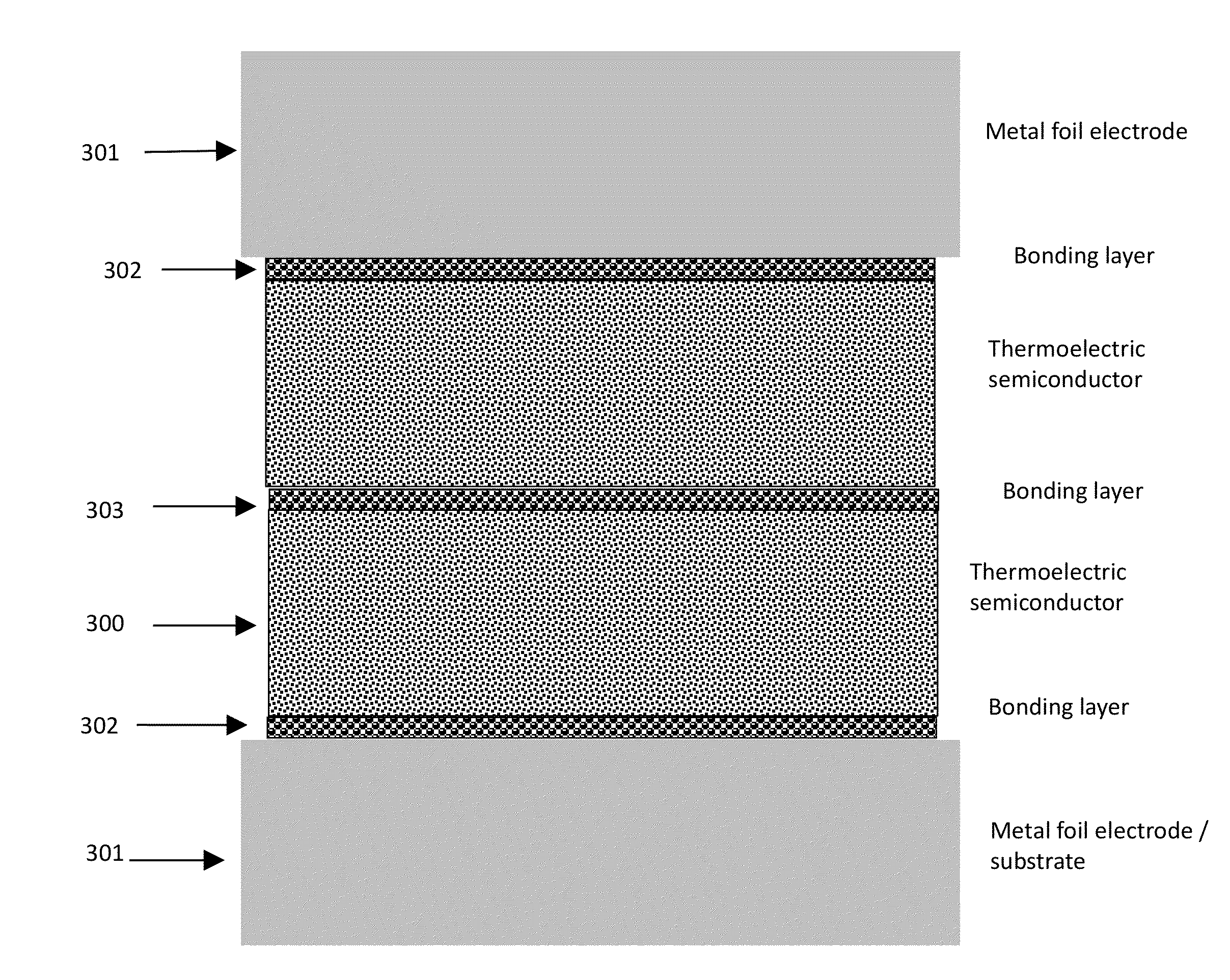
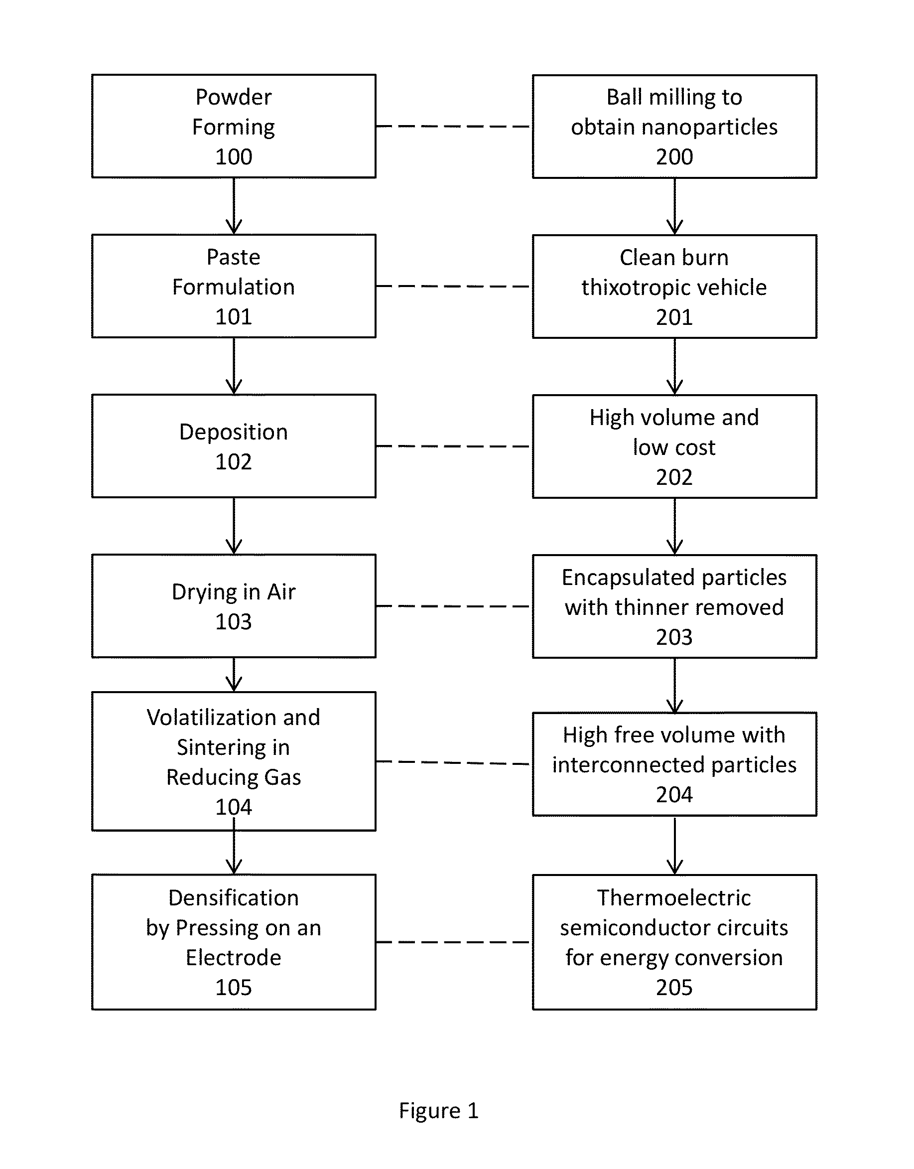
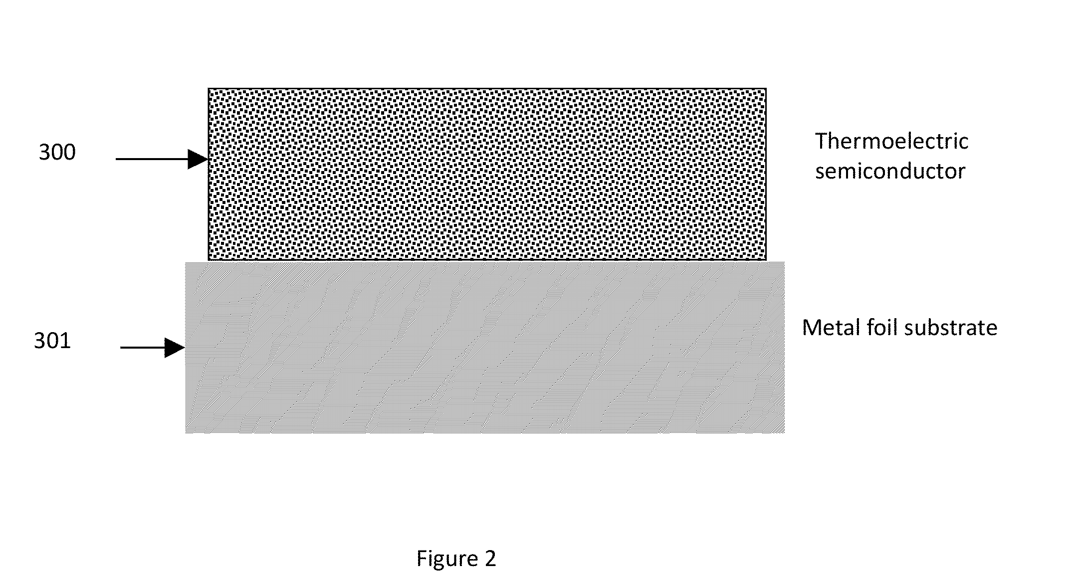
[0041]FIG. 1 is an illustration of the discrete process steps relevant to the present invention. Such a process would lead to a progression to discrete thermoelectric devices and modules for energy conversion in high volume production, since thick film technology by screen or stencil printing is well-established. As provided by Min, the thicknesses of discrete p or n type devices for thermoelectric applications can be chosen for maximum power or maximum efficiency. For energy harvesting from heat, the choice is to design in accordance with maximum power, which requires devices that are thinner than those for maximum conversion efficiency. Discrete devices can be fabricated by either a semiconductor ‘pellet’ [U.S. Pat. No. 5,318,743] or thick film screen printing as given in the several publications cited. P...


PUM

PropertyMeasurementUnit
temperatureaaaaaaaaaa
thicknessaaaaaaaaaa
thicknessaaaaaaaaaa

Abstract

Solid state thermoelectric energy conversion devices can provide electrical energy from heat flow, creating energy, or inversely, provide cooling through applying energy. Thick film methods are applied to fabricate thermoelectric device structures using microstructures formed through deposition and subsequent thermal processing conditions. An advantageous coincidence of material properties makes possible a wide variety of unique microstructures that are easily applied for the fabrication of device structures in general. As an example, a direct bond process is applied to fabricate thermoelectric semiconductor thick films on substrates by printing and subsequent thermal processing to form unique microstructures which can be densified. Bismuth and antimony are directly bonded to flexible nickel substrates.

Description

CROSS-REFERENCE TO RELATED APPLICATIONS[0001]This application claims priority to U.S. provisional application No. 61 / 759,983, filed Feb. 1, 2013, the contents of which are hereby incorporated herein selectively.U.S. PATENT DOCUMENTSU.S. Pat. No. 4,902,648February 1990Ohta et alU.S. Pat. No. 5,103,286April 1992Ohta et alU.S. Pat. No. 5,108,515April 1992Ohta et alU.S. Pat. No. 5,246,504September 1993Ohta et alU.S. Pat. No. 5,318,743June 1994Tokiai et alU.S. Pat. No. 5,817,188October 1998Yahatz et alU.S. Pat. No. 6,100,463August 2000Ladd et alU.S. Pat. No. 6,103,967August 2000Cauchy et al.OTHER PUBLICATIONS[0002]Walton, Principles of thick film materials formulation, The Radio and Electronic Engineer, Vol. 45, No. 3, March 1975, p. 139-143[0003]Min, Thermoelectric Module Design Theories, Rowe, David Michael, ed. Thermoelectrics Handbook: Macro to Nano, CRC press, 2006, Ch. 11[0004]Ohta et al, Characteristics of (Bi, Sb)2 (Te, Se)3 Based Thick-Film Thermoelectric Elements for Power Gene...

Claims


Application Information

Patent Timeline
Patent Type & Authority Applications(United States)
IPC IPC(8): H01L35/34
CPCH01L35/34H10N10/852H10N10/853H10N10/01H10N10/17C23C28/00C23C30/00C23C24/082
Inventor PETKIE, RONALD R.
Owner ATS IP LLC
Why Eureka
Try Eureka