Nitride semiconductor light emitting device

Active Publication Date: 2014-10-30
INTELLECTUAL DISCOVERY CO LTD
View PDF3 Cites 13 Cited by
  • Summary
  • Abstract
  • Description
  • Claims
  • Application Information

AI Technical Summary

Benefits of technology

[0010]Therefore, the technical problem of the present invention is to provide a nitride semiconductor light emitting device with improved light efficiency in which a hole injection efficiency from p-type nitride laye

Problems solved by technology

However, there is a problem that a hole injection efficiency is decreased since the is electron blocking lay

Method used


Image

  • Nitride semiconductor light emitting device
  • Nitride semiconductor light emitting device
  • Nitride semiconductor light emitting device

Examples


Embodiment Construction

[0027]The present invention is described more fully hereinafter with reference to the accompanying drawings, in which example embodiments of the present invention are shown. The present invention may, however, be embodied in many different forms and should not be construed as limited to the example embodiments set forth herein. Rather, these example embodiments are provided so that this disclosure will be thorough and complete, and will fully convey the scope of the present invention to those skilled in the art. In the drawings, the sizes and relative sizes of layers and regions may be exaggerated for clarity.

[0028]Hereinafter, exemplary embodiments of the present invention will be described in detail with reference to the accompanying drawings.

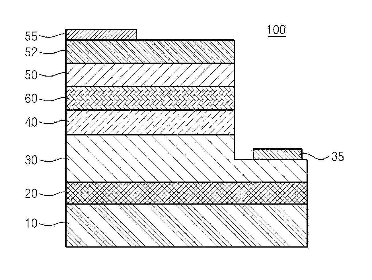
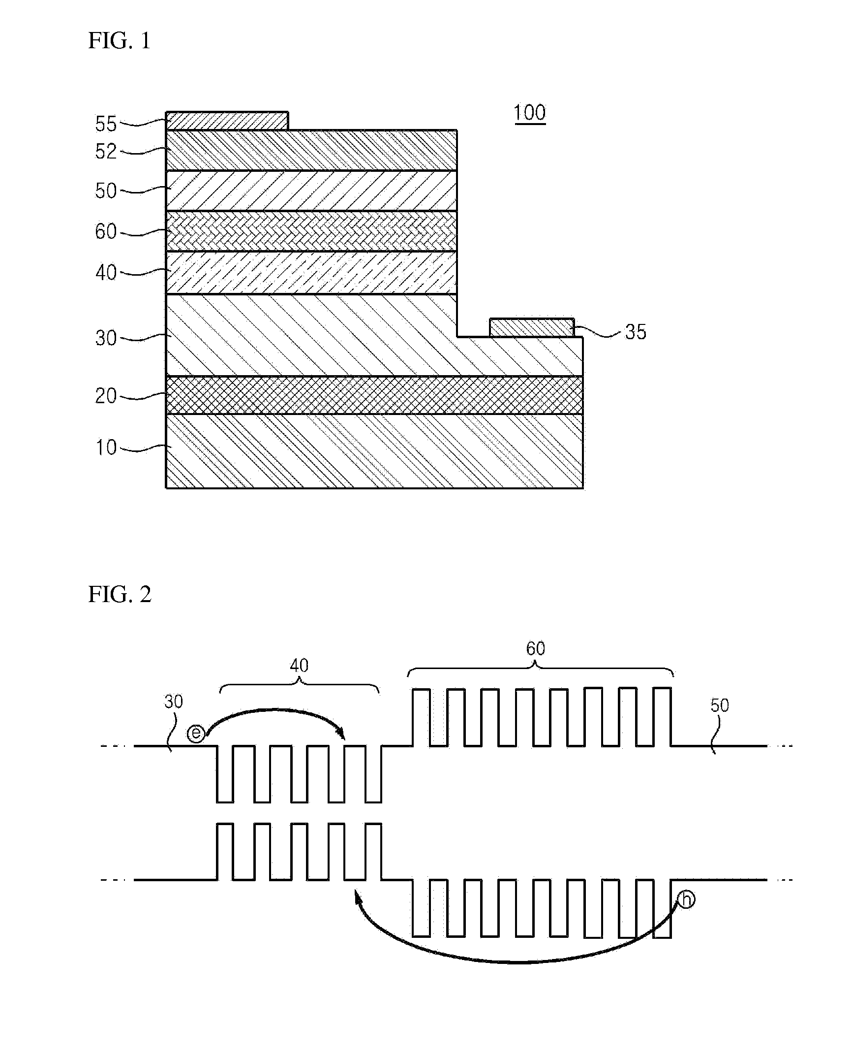
[0029]FIG. 1 is a cross sectional view of a light emitting device.

[0030]As shown in FIG. 1, a nitride semiconductor light emitting device 100 comprises a substrate 10, a buffer layer 20, a n-type nitride layer 30, a n-type electrode 35, an ac...


PUM


Abstract

The present invention discloses a nitride semiconductor light emitting device with improved light efficiency. The nitride semiconductor light emitting device includes a n-type nitride layer and p-type nitride layer, an active layer disposed between the n-type and p-type nitride layers and with a multiple quantum well structure wherein a plurality of quantum well layers and a plurality of quantum barrier layers are stacked alternatively in the active layer, and a superlattice layer between the active layer and the p-type nitride layer with asymmetric structure. Herein, a thickness of a well layers gradually increases from the p-type nitride layer to the active layer and the height of the barrier layers gradually increases from the active layer to the p-type nitride layer and therefore, an injection efficiency of a hole supplied from p-type nitride layer to an active layer is increased.

Description

CROSS REFERENCE TO RELATED APPLICATION[0001]This application claims priority from and the benefit of Korean Patent Application No. 10-2013-0032105 filed on Mar. 26, 2013, which is hereby incorporated by reference for all purposes as if fully set forth herein.BACKGROUND OF THE INVENTION[0002]1. Field of the Invention[0003]The present invention relates to a nitride semiconductor light emitting device with improved light efficiency, more specifically to a nitride semiconductor light emitting device with improved light efficiency in which a hole injection efficiency from a p-type nitride layer to an active layer is improved through forming a superlattice layer with asymmetrical structure by changing a thickness of well layers or a height of barrier layers between an active layer and p-type nitride layer.[0004]2. Discussion of the Background[0005]In general, III elements such as Gallium Nitride (GaN), Aluminum Nitride (AlN), and Indium Gallium Nitride (InGaN) used for a nitride semicondu...

Claims


Application Information

Patent Timeline
IPC IPC(8): H01L33/06H01L33/32
CPCH01L33/32H01L33/06H01L33/04H01L33/14
Inventor PARK, SEONG-JULEE, SANG-JUNHONG, SANG-HYUNKIM, SANG-JO
Owner INTELLECTUAL DISCOVERY CO LTD
Why Eureka
Try Eureka