
Integrated circuits with laterally diffused metal oxide semiconductor structures

a metal oxide semiconductor and integrated circuit technology, applied in the field of integrated circuits, can solve the problems of limiting the performance of these devices, affecting the performance and reliability of devices, and localized and non-uniform buildup of interface states and oxide charges, so as to achieve the effect of improving the structure of ldmos

Active Publication Date: 2014-10-30
GLOBALFOUNDRIES SINGAPORE PTE LTD
View PDF6 Cites 26 Cited by
  • Summary
  • Abstract
  • Description
  • Claims
  • Application Information

AI Technical Summary

Benefits of technology

The patent text describes integrated circuits with improved LDMOS structures. These circuits include a semiconductor substrate, shallow trench isolation regions, and a transistor structure. The circuit also includes two gate electrodes and a source region. The method of operation involves applying different voltages to the two gate electrodes. The technical effect is improved performance and reliability of the integrated circuits.

Problems solved by technology

Hot carrier injection” (HCI) degradation can significantly limit the performance of these devices, particularly when operating in a saturation region.
This injection of charge carriers often results in a localized and non-uniform buildup of interface states and oxide charges near and underneath a gate and / or in the drift region of the device.
For example, HCI can produce variations in certain characteristics of the LDMOS device, including saturation current, threshold voltage, transconductance, on-resistance, etc., thus undesirably affecting the performance and reliability of the device.
Locating the LDD region in close relative proximity to the silicon / oxide interface, however, significantly increases the likelihood that charged carriers will become trapped at the interface, thereby increasing HCI degradation in the device.
However, since the LDD region is typically formed at the silicon / oxide interface of the device, as previously stated, increasing the doping concentration of the LDD region also undesirably increases HCI degradation in the device.
The increase in HCI degradation resulting from the increased doping concentration of the LDD region often significantly undermines any beneficial reduction in on-resistance that may otherwise be achieved by increasing the doping concentration of the LDD region.
Furthermore, by increasing the doping concentration of the LDD region in the device, a breakdown voltage of the device is undesirably reduced.

Method used


Image

  • Integrated circuits with laterally diffused metal oxide semiconductor structures
  • Integrated circuits with laterally diffused metal oxide semiconductor structures
  • Integrated circuits with laterally diffused metal oxide semiconductor structures

Examples


Embodiment Construction

[0015]The following detailed description is merely exemplary in nature and is not intended to limit the various embodiments or the application and uses thereof. Furthermore, there is no intention to be bound by any theory presented in the preceding background or the following detailed description.

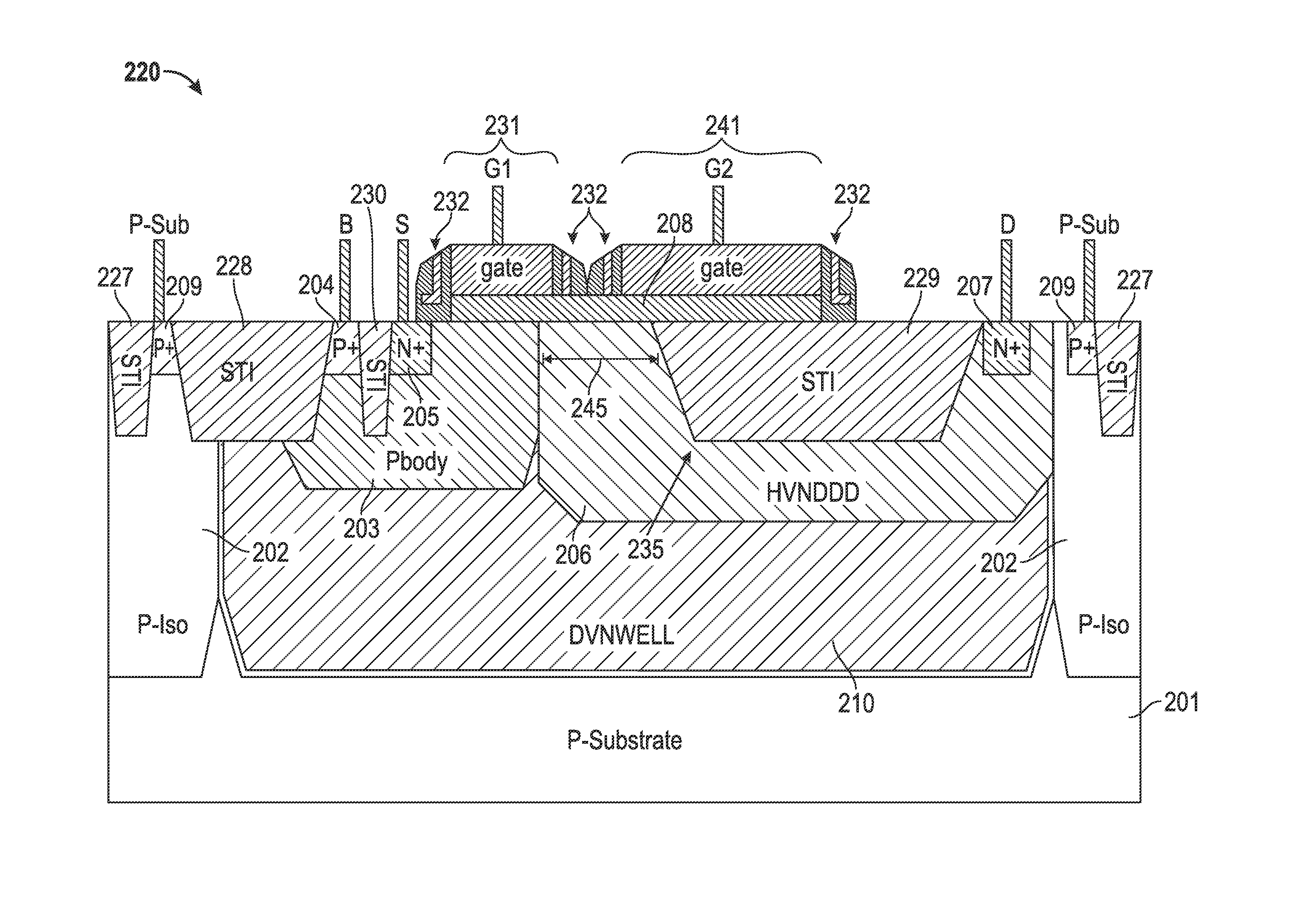
[0016]Various embodiments of an LDMOS integrated circuit are described herein. The embodiments utilize a dual gate electrode to form the LDMOS structure, with a differential voltage applied between each gate electrode. The described embodiments reduce the impact of the HCI phenomenon, thereby allowing the LDMOS integrated circuits to be operated at more desirable voltage and current levels.

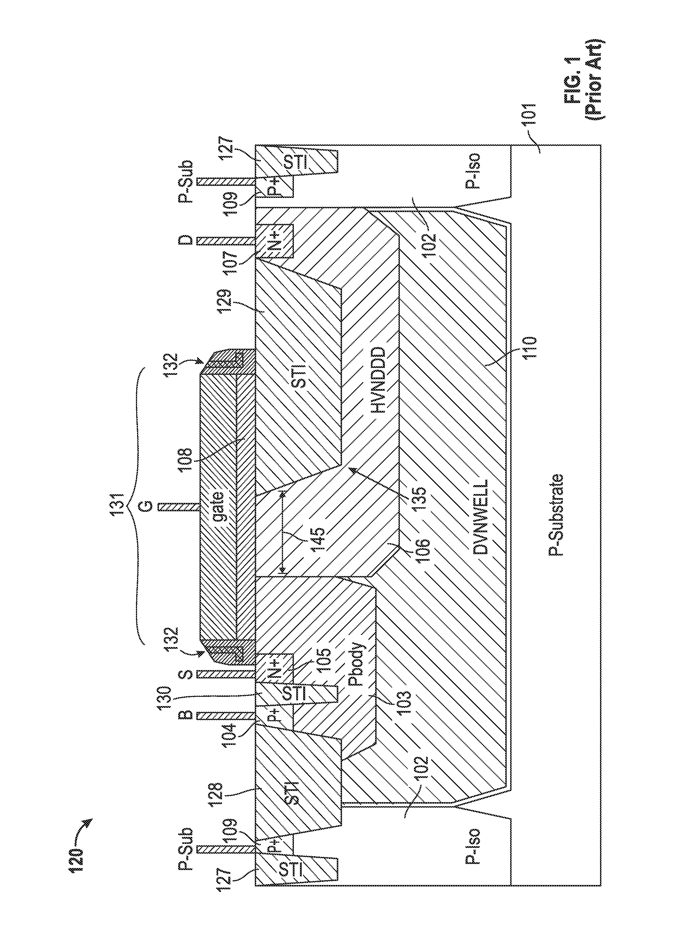
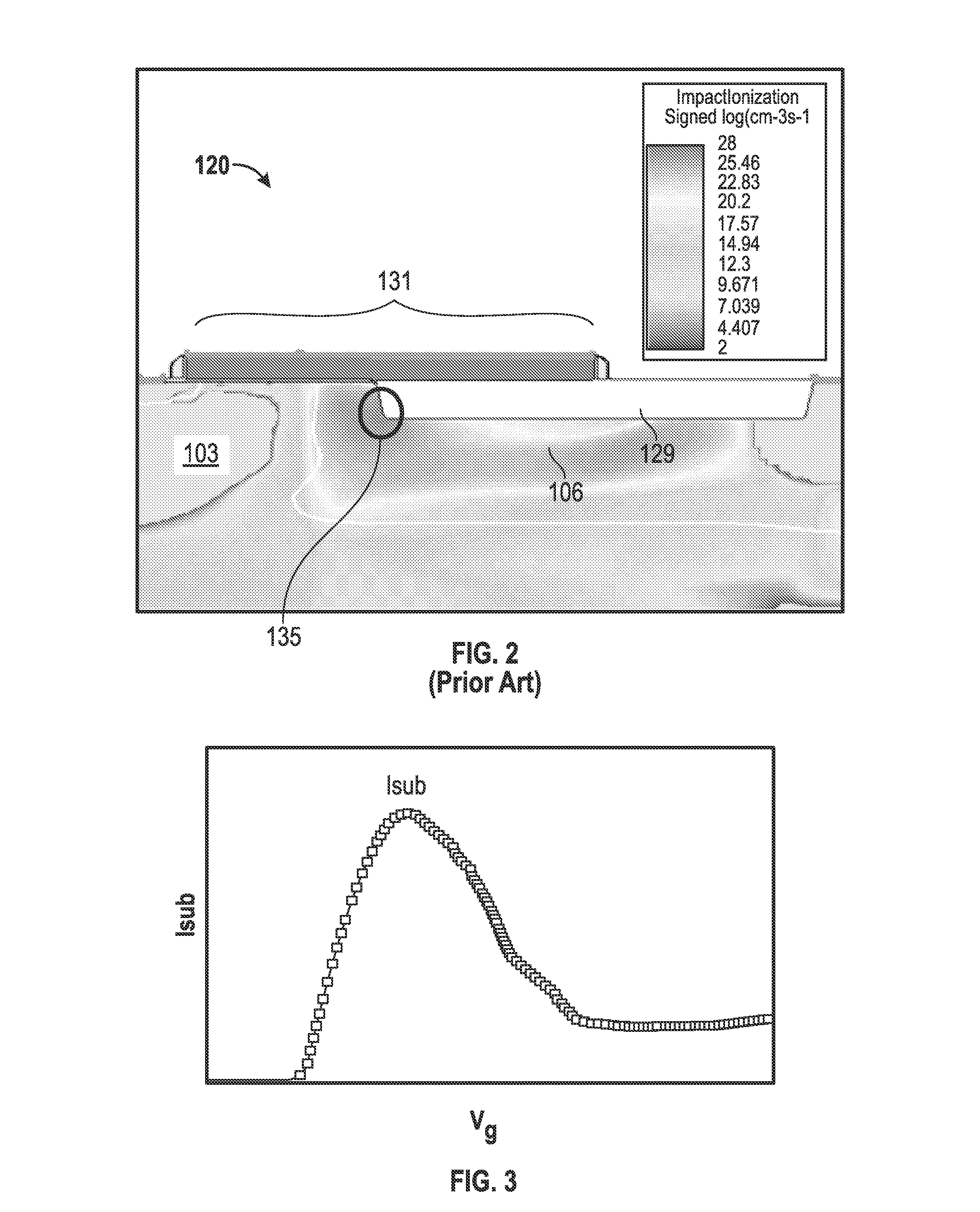
[0017]FIG. 1 is a cross sectional view of a conventional LDMOS transistor 120, provided for purposes of comparison with the present invention, which includes P− substrate 101, primary n-well regions 110, deep p-well region 103, P+ backgate contact 104, N+ source region 105, n-type reduced surface field re...


PUM


Abstract

Integrated circuits with improved LDMOS structures are provided. An integrated circuit includes a semiconductor substrate, a plurality of shallow trench isolation (STI) regions, each extending at least a first depth below an upper surface of the semiconductor substrate. The STI regions electrically isolate devices fabricated in the semiconductor substrate. The integrated circuit further includes a transistor structure. The transistor structure includes a gate dielectric positioned over a portion of a first one of the plurality of STI regions, a drain region adjacent to the first one of the plurality of STI regions and spaced apart from the gate dielectric, a first gate electrode that extends over a first portion of the gate dielectric, a second gate electrode that extends over a second portion of the gate dielectric and positioned adjacent to the first gate electrode, and a source region positioned adjacent to the first portion of the gate dielectric.

Description

TECHNICAL FIELD[0001]The technical field generally relates to integrated circuits, and more particularly relates to laterally diffused metal oxide semiconductor integrated circuits.BACKGROUND[0002]Power MOS devices, including lateral diffused MOS (LDMOS) devices, are employed in a wide variety of applications, such as, for example, power amplifiers in wireless communications systems. “Hot carrier injection” (HCI) degradation can significantly limit the performance of these devices, particularly when operating in a saturation region. As is well known, the HCI phenomenon generally results from heating and subsequent injection of charge carriers into the gate oxide and / or an oxide layer above a drift region of an LDMOS device. This injection of charge carriers often results in a localized and non-uniform buildup of interface states and oxide charges near and underneath a gate and / or in the drift region of the device. For example, HCI can produce variations in certain characteristics of...

Claims


Application Information

Patent Timeline
IPC IPC(8): H01L29/78H03K3/01H01L27/088
CPCH01L29/7816H03K3/01H01L27/088H01L29/0649H01L29/0878H01L29/1087H01L29/402H01L29/6656H01L29/66689
Inventor LU, YIWANG, DONGLICHEN, DEYANVERMA, PURAKH RAJ
Owner GLOBALFOUNDRIES SINGAPORE PTE LTD
Learn More