Semiconductor device

Active Publication Date: 2014-10-30
FUJI ELECTRIC CO LTD
View PDF1 Cites 16 Cited by
  • Summary
  • Abstract
  • Description
  • Claims
  • Application Information

AI Technical Summary

Benefits of technology

[0023]As explained hereinabove, in the semiconductor device in accordance with the present invention, a set signal and a reset signal for controlling a high-potential-side switching element are transmitted by modulation and demodulation with a single level shift circuit. Therefore, the effect of dV/dt noise or the like can be reduced and a malfunction caused by a spread in characteristics of devices, which occurs

Problems solved by technology

However, the techniques described in the aforementioned Patent Document 1 and Patent Document 2 each use two level shift circuits, one on the set side and one on the reset side, an out-of-synch operation caused by a spread in characteri

Method used


Image

  • Semiconductor device
  • Semiconductor device
  • Semiconductor device

Examples


Example

[0041]A semiconductor device according to an example of the present invention will be explained below with reference to the appended drawings. Examples described hereinbelow are the preferred specific examples of the semiconductor device in accordance with the present invention, and although those examples may have various technically preferred limitations, the technical scope of the present invention is not limited to those examples, unless specifically indicated otherwise. The constituent elements in the embodiment described hereinbelow can be replaced, as appropriate, by the presently available constituent elements, and a variety of combinations with other already available constituent elements can be also used. Therefore, the contents of the invention set forth in the claims are not limited to the description of the embodiment.

(Configuration of Semiconductor Device)

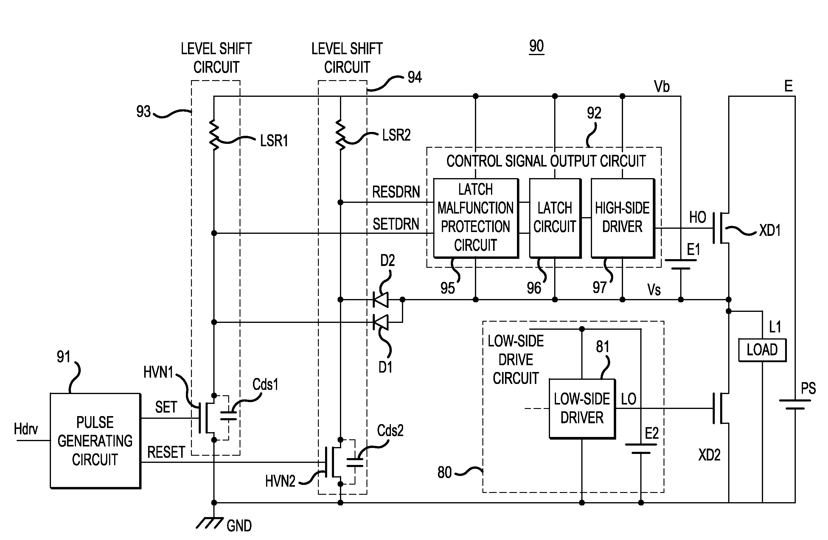
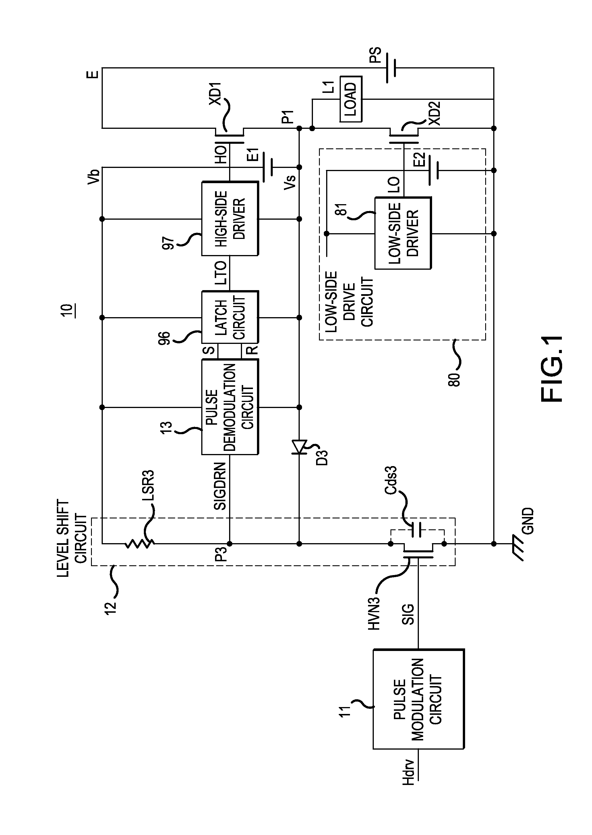
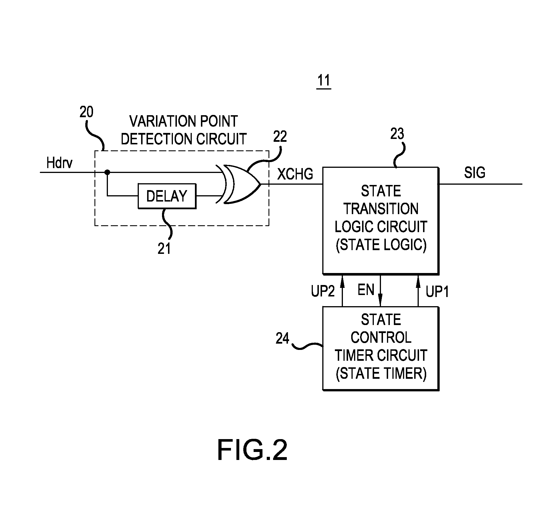
[0042]FIG. 1 is a block diagram of a high-side drive circuit 10 as an example of the semiconductor device according...


PUM


Abstract

In aspects of the invention, a semiconductor device can include one level shift circuit that outputs a low-side input signal as a high-side signal upon raising a signal level, a pulse modulation circuit that operates in a low-side region, generates a data symbol constituted by or more bits and representing a set signal or a reset signal, where bit is defined as a combination of codes forming a pair. The pulse generation circuit can output the generated data symbol as an input signal of the level shift circuit. Also included can be a pulse demodulation circuit that operates in a high-side region, demodulates the data symbol outputted from the level shift circuit and generates a level-shifted set signal or reset signal; and a control circuit that controls conduction/non-conduction of the high-potential-side switching element on the basis of the level-shifted set signal or reset signal outputted from the pulse demodulation circuit.

Description

CROSS-REFERENCE TO RELATED REFERENCES[0001]This application is a continuation of International Application No. PCT / JP 2013 / 051109, filed on 21 Jan. 2013, which is based on and claims priority to Japanese Patent Application No. JP 2012-084069, filed on 2 Apr. 2012. The disclosure of the Japanese priority application and the PCT application in their entirety, including the drawings, claims, and the specification thereof, are incorporated herein by reference.BACKGROUND[0002]1. Field of the Invention[0003]Embodiments of the invention relate to semiconductor devices that can be used in a half-bridge power source and have a level shift circuit.[0004]2. Related Art[0005]The circuit of a half-bridge power source or the like is typically configured as shown in FIG. 15. This circuit is provided with an output circuit 60 in which a high-potential-side switching element XD1 and a low-potential-side switching element XD2 are connected in series. An input buffer and protection circuit 70 that gen...

Claims


Application Information

Patent Timeline
IPC IPC(8): H03K17/082H03K19/0175H03K3/012H03K17/22
CPCH03K17/0822H03K3/012H03K19/017509H03K17/22H03K7/08H03K9/08H03K17/162H03K2217/0063
Inventor AKAHANE, MASASHI
Owner FUJI ELECTRIC CO LTD
Why Eureka
Try Eureka