Time-to-digital conversion with analog dithering

a technology of analog dithering and time-to-digital conversion, which is applied in the field of phaselocked loop (pll) devices, can solve the problems of high power consumption for the generation and processing of clock signals, measurement errors at the beginning and end of time intervals, and quantization noise can still appear at low frequencies

Active Publication Date: 2014-10-30
ASAHI KASEI ELECTRONICS CO LTD
View PDF11 Cites 10 Cited by
  • Summary
  • Abstract
  • Description
  • Claims
  • Application Information

AI Technical Summary

Benefits of technology

[0030]In some embodiments, generating the supply voltage of the delay elements of the TDC supply voltage generator comprises digital-to-analog converting the dithering signal; low-pass filtering the analog translated dithering signal; and generating the TDC supply voltage with respect to the low pass filtered analog translated dithering signal.
[0031]In some embodiments, low-pass filtering the analog translated dithering signal is carried out using a programmable low-pass filter configured to convert a time interval between an active edge of a first signal and an active edge of a second signal into a binary output value, comprises a time-to-digital converter, TDC, comprising an arrangement of a number Q of cascaded delay elements (G1-GQ) each having a propagation delay that exhibits a dependency to a supply voltage, the arrangement receiving the first signal in input; a set of Q sampling elements configured to generate Q sample values by sampling respective outputs of the Q delay elements responsive to the active edge of a second signal; an encoder configured to generate the binary output value (TDC_output) from the Q sample values; and a dithering arrangement comprising a digital dithering signal generator, configured to generate a dithering signal (DS) in the digital domain; and a supply voltage generator configured to generate the supply voltage of the delay elements of the TDC, with respect to the dithering signal.

Problems solved by technology

This causes a measurement error at the beginning and at the end of the time interval.
However, increasing the clock frequency results in higher power consumption for the generation and processing of the clock signal.
However, some quantization noise can still appear at low frequencies because of imperfect noise shaping.
An expected drawback of this solution, however, is that the added noise can be significantly stronger than the intrinsic analog performance of the TDC.

Method used


Image

  • Time-to-digital conversion with analog dithering
  • Time-to-digital conversion with analog dithering
  • Time-to-digital conversion with analog dithering

Examples


Embodiment Construction

[0045]Reference will now be made in detail to embodiments, examples of which are illustrated in the accompanying drawings. In the following detailed description, numerous non-limiting specific details are set forth in order to assist in understanding the subject matter presented herein. It will be apparent, however, to one of ordinary skill in the art that various alternatives may be used without departing from the scope of the present invention and the subject matter may be practiced without these specific details.

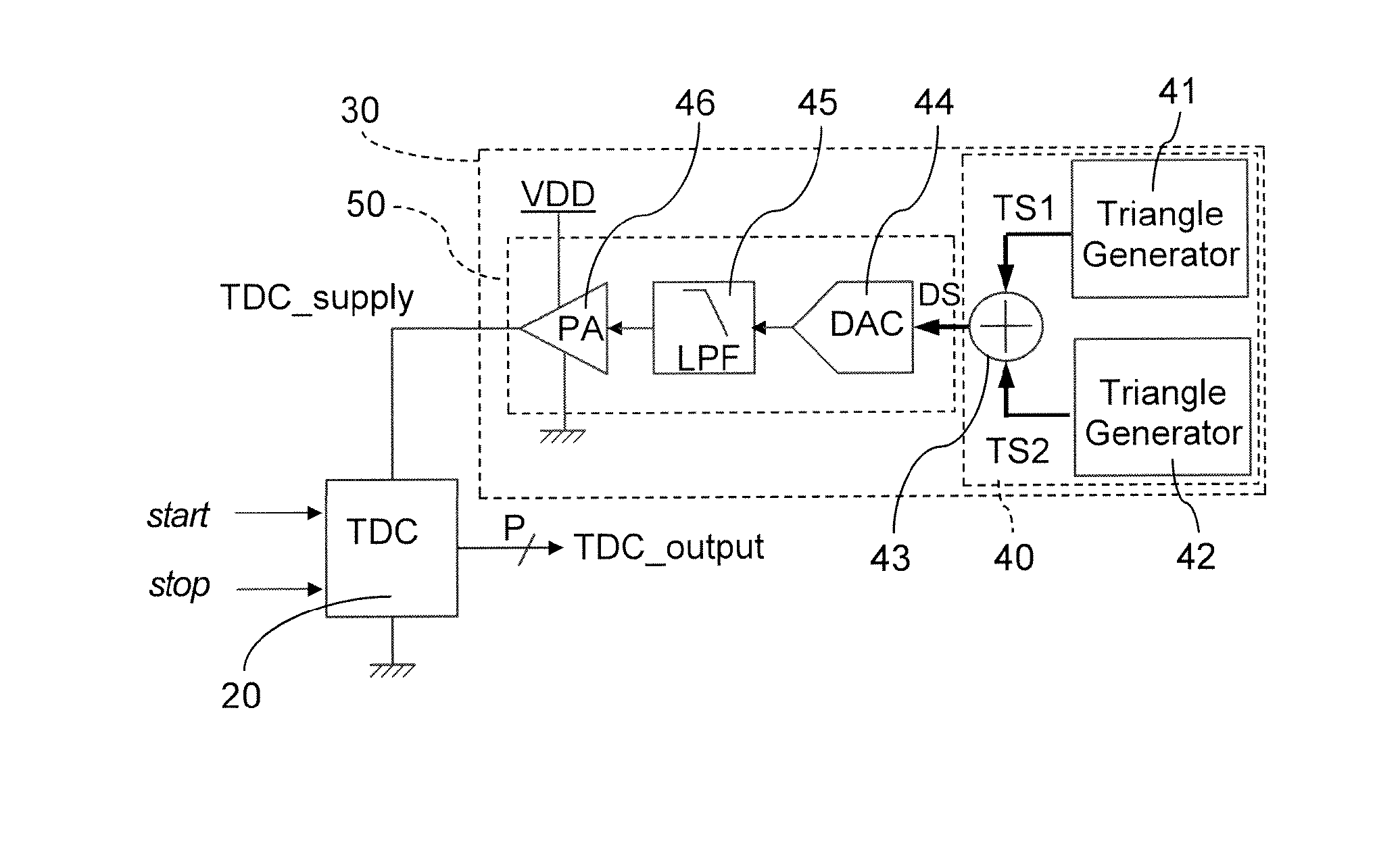
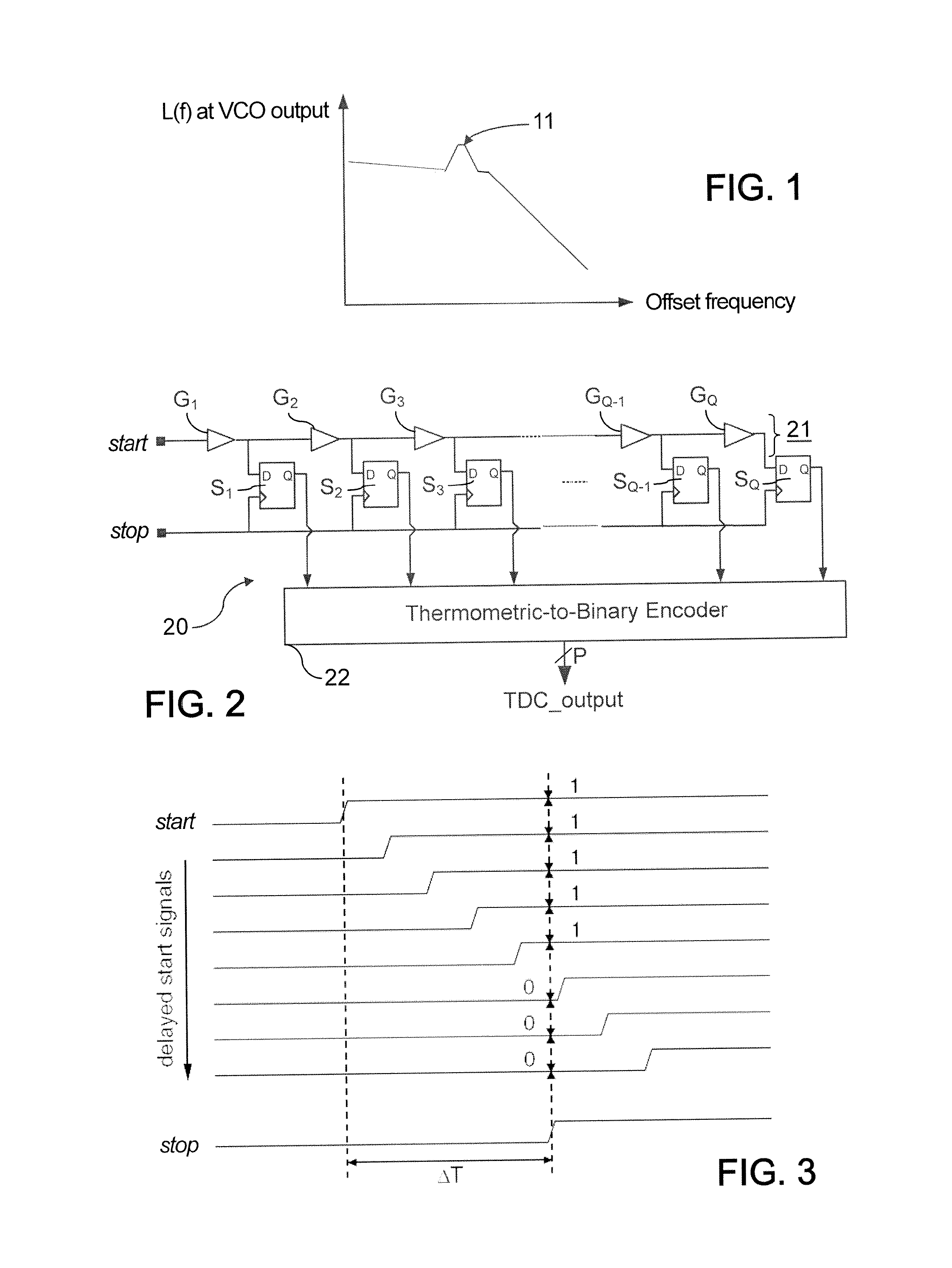
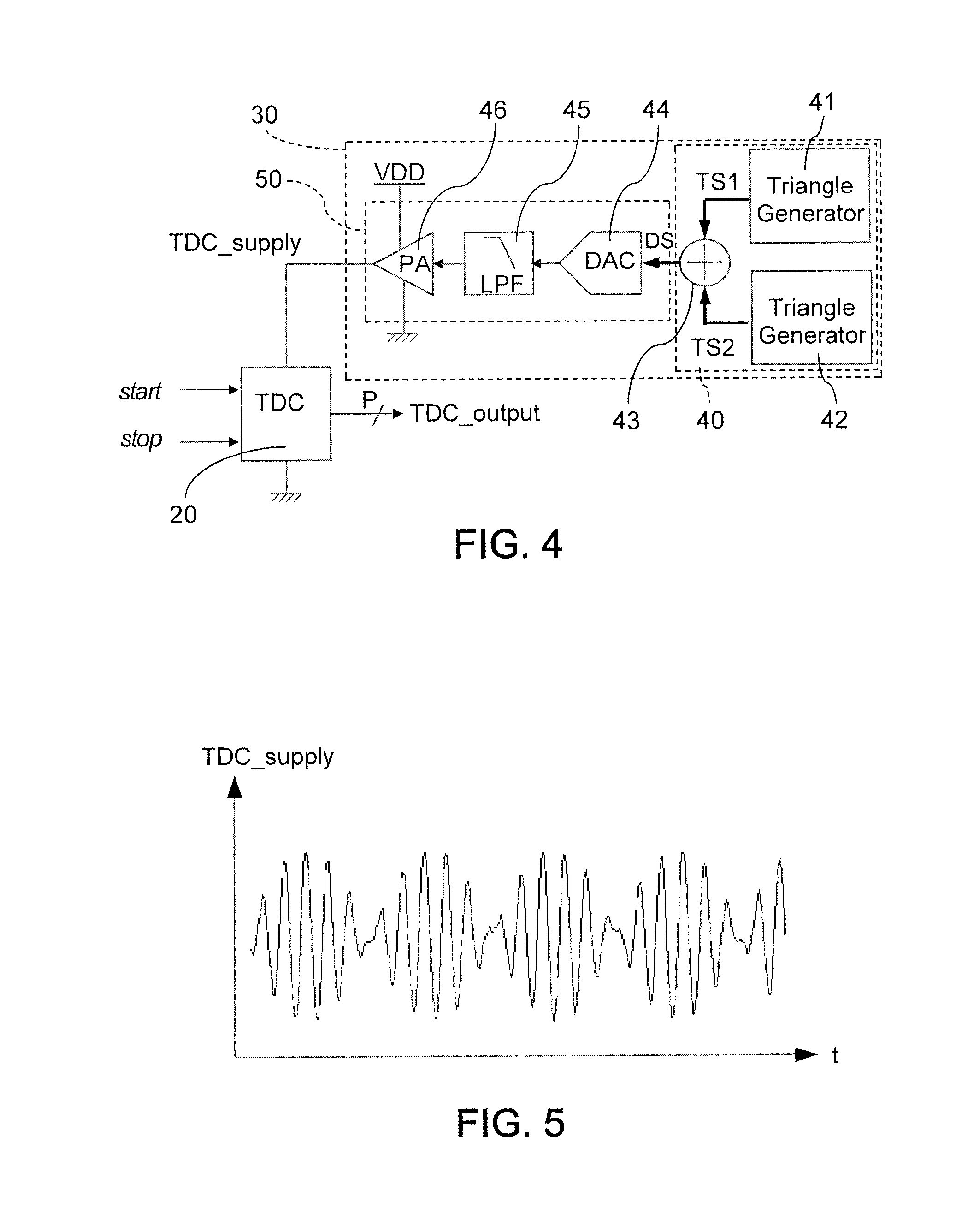
[0046]Referring to FIG. 2, there is shown therein a schematic circuit diagram of an example of a Time-to-Digital Converter (TDC) 20 to which embodiments of the invention may be applied. The TDC is based on a tapped delay-line structure 21, in which the start signal is fed. The start signal is the signal carrying the time information to be converted.

[0047]The tapped delay-line 21 contains a number Q of delay elements, or cells, each introducing an elementary delay time r. ...


PUM


Abstract

There is described a time-to-digital conversion scheme using an arrangement of delay elements based Time-to-Digital Converter, TDC (20), wherein dithering is built in the digital domain and introduced in the analog domain as a modulation of a supply voltage (TDC-supply) supplying delay elements of the TDC, each having a propagation delay which exhibits a dependency to their supply voltage.

Description

[0001]This application claims the priority and benefit of European patent no. 13305539.2 to Asahi Kasei Microdevices Corporation of Japan, entitled “Time-To-Digital Conversion With Analog Dithering,” filed Apr. 24, 2013, which is hereby incorporated by reference in its entirety.TECHNICAL FIELD[0002]The invention relates generally to a phase-locked loop (PLL) device that is provided with synchronization capabilities. The invention also relates to processes for operating such a PLL device, and operating simultaneously several such PLL devices.BACKGROUND OF THE INVENTION[0003]The approaches described in this section could be pursued, but are not necessarily approaches that have been previously conceived or pursued. Therefore, unless otherwise indicated herein, the approaches described in this section are not prior art to the claims in this application and are not admitted to be prior art by inclusion in this section.[0004]A Time-to-Digital Converter (TDC) is an electronic device common...

Claims


Application Information

Patent Timeline
Patent Type & Authority Applications(United States)
IPC IPC(8): H03M1/20H03L7/093
CPCH03L7/093H03M1/201G04F10/005H03L7/085H03L7/18
Inventor CANARD, DAVIDDELORME, JULIEN
Owner ASAHI KASEI ELECTRONICS CO LTD
Why Eureka
Try Eureka