Flexible light emitting semiconductor device having a three dimensional structure

a technology of light-emitting semiconductors and three-dimensional structures, which is applied in the direction of fixed installation, lighting and heating equipment, lighting support devices, etc., and can solve problems such as heat managemen

Active Publication Date: 2014-10-30
3M INNOVATIVE PROPERTIES CO
View PDF5 Cites 36 Cited by
  • Summary
  • Abstract
  • Description
  • Claims
  • Application Information

AI Technical Summary

Benefits of technology

[0006]At least one aspect of the present invention provides a cost-effective thermal management solution for current and future high power LESD constructions through a robust flexible LESD construction. The ability to dissipate large amounts of heat is needed for the operation of high power LESD arrays. According to at least one embodiment of the present invention, heat dissipation can be managed by integrating the LESDs into a system having a flexible polymeric dielectric substrate, i.e., a dielectric layer. To accomplish better heat management, LESDs are positioned so they are in close or direct thermal contact with thermally conductive layers by controlling the thickness of the insulator (dielectric) material between the LESD and a thermally conductive layer or by completely removing the insulator material between the LESD and a thermally conductive layer. In at least one embodiment of the present invention, to achieve the desired positioning of the LESD controlled removal, e.g., by etching, of the dielectric layer to a desired thickness to form a cavity, or creating an opening completely through the dielectric layer to form a via, is performed. Etching of the dielectric layer may provide additional advantages by creating slanted side walls which can be coated with a reflecting material to provide enhanced light efficiency. Additionally, in at least some embodiments, because the LESD sits below the surface of the dielectric layer, it has a lower profile than standard LES devices, which makes it well-suited for low form factor applications.
[0011]Another advantage of at least one embodiment of the present invention is that the cavity or via contains the encapsulant filling in a confined area. Another advantage of at least one embodiment of the present invention is that the LESDs on the flexible dielectric layer may be electrically connected in series, in parallel, or individually depending on the desired application. Another advantage of at least one embodiment of the present invention is that the flexible dielectric layer facilitates making a circuitry pattern on both sides of the substrate. Another advantage of at least one embodiment of the present invention is that the flexible substrate provides great flexibility and bendability for the LESD articles.

Problems solved by technology

A common issue with light-producing articles such as those containing LEDs is heat management.

Method used


Image

  • Flexible light emitting semiconductor device having a three dimensional structure
  • Flexible light emitting semiconductor device having a three dimensional structure
  • Flexible light emitting semiconductor device having a three dimensional structure

Examples


Embodiment Construction

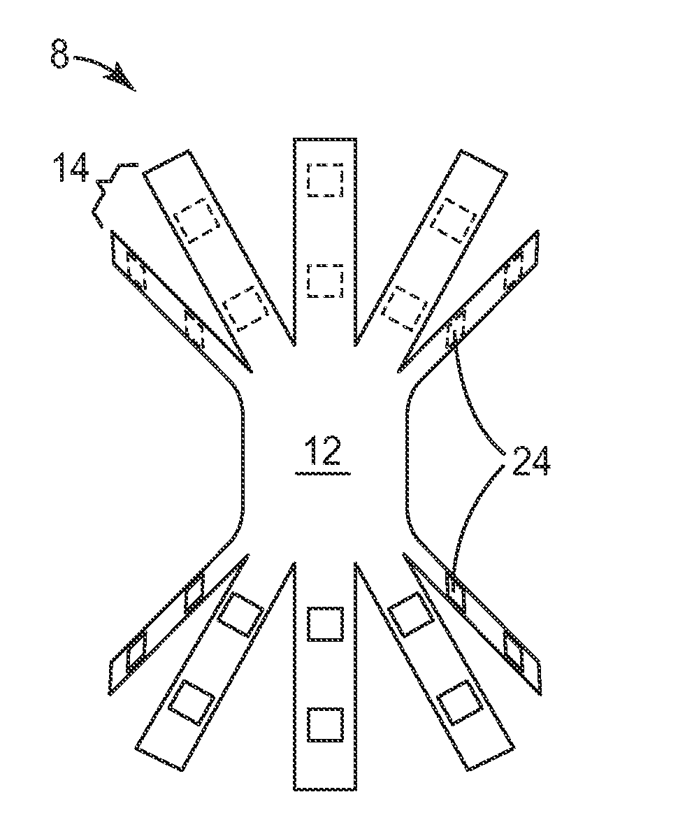
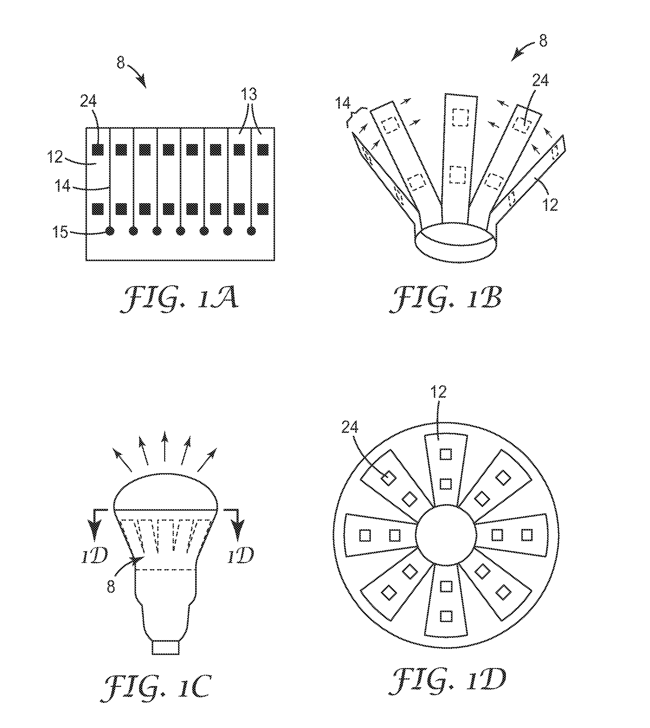
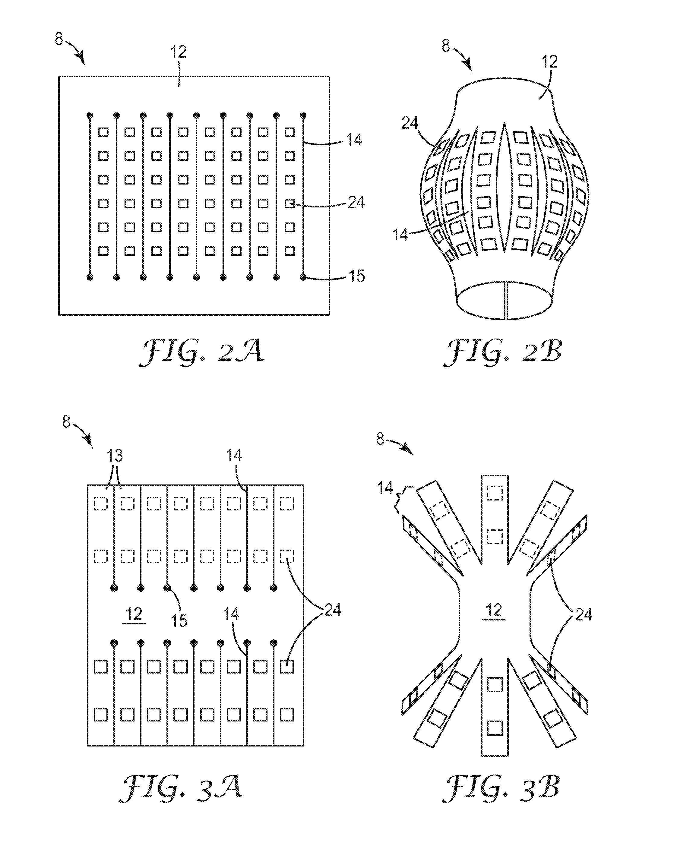
[0025]In the following description, reference is made to the accompanying set of drawings that form a part of the description hereof and in which are shown by way of illustration several specific embodiments. In general similar reference numbers are used for similar features in the various embodiments. Unless indicated otherwise, these similar features may comprise the same materials, have the same attributes, and serve the same or similar functions. Additional or optional features described for one embodiment may also be additional or optional features for other embodiments, even if not explicitly stated, where appropriate. It is to be understood that other embodiments are contemplated and may be made without departing from the scope or spirit of the present invention. The following detailed description, therefore, is not to be taken in a limiting sense.

[0026]Unless otherwise indicated, all numbers expressing feature sizes, amounts, and physical properties used in the specification...


PUM


Abstract

Provided is an article comprising a flexible circuit comprising a polymeric dielectric layer having first and second major surfaces, one or both of the first and second major surfaces having a conductive layer thereon, wherein at least one conductive layer comprises an electrical circuit configured to power one or more light emitting semiconductor devices located on the flexible circuit, wherein the flexible circuit is shaped to form a three dimensional structure.

Description

TECHNICAL FIELD[0001]This invention relates to flexible light emitting semiconductor devices.BACKGROUND[0002]Conventional light emitting semi-conductor (LES) devices (LESDs), including light emitting diodes (LEDs) and laser diodes, and packages containing LESDs have several drawbacks. High power LESDs generate a substantial amount of heat that must be managed. Thermal management deals with problems arising from heat dissipation and thermal stresses, which is currently a key factor in limiting the performances of light-emitting diodes.[0003]In general, LES devices are commonly prone to damage caused by a buildup of heat generated from within the devices, as well as heat from sunlight in the case of outside lighting applications. Excessive heat buildup can cause deterioration of the materials used in the LES devices, such as encapsulants for the LESDs. When LESDs are attached to flexible-circuit laminates, which may also include other electrical components, the heat dissipation proble...

Claims


Application Information

Patent Timeline
Patent Type & Authority Applications(United States)
IPC IPC(8): F21V21/14F21V29/00F21K99/00F21W107/00
CPCF21V21/14F21V29/004F21K9/00H01L25/0753F21V3/00F21W2121/00H05K1/028H05K1/189H05K2201/047H05K2201/053H05K2201/09063H05K2201/10106H01L2924/0002F21K9/232F21Y2115/10F21Y2107/00F21Y2107/40F21W2107/00H01L2924/00F21S2/005F21V23/003H01L33/10H01L33/56F21V29/70
Inventor NARAG, ALEJANDRO ALDRIN II AGCAOILIPALANISWAMY, RAVIJESUDOSS, AROKIARAJMOONEY, JUSTINE A.
Owner 3M INNOVATIVE PROPERTIES CO
Why Eureka
Try Eureka