NANO field-effect vacuum tube and fabrication method thereof

a vacuum tube and nano-field technology, applied in the field of nano-field-effect vacuum tubes and fabrication techniques thereof, can solve the problems of unstable performance difficult fabrication of existing vacuum tubes, and difficult integration of vacuum tubes with other devices

Active Publication Date: 2014-11-13
SEMICON MFG INT (SHANGHAI) CORP
View PDF12 Cites 11 Cited by
  • Summary
  • Abstract
  • Description
  • Claims
  • Application Information

AI Technical Summary

Benefits of technology

The present disclosure includes a method for fabricating a nano field-effect vacuum tube that is easy to integrate with existing integrated circuits. The method includes steps of forming a sacrificial layer, a source sacrificial layer, and a drain sacrificial layer on a substrate having an insulating layer. A trench is then formed in the insulating layer, followed by the formation of a dielectric layer on the sacrificial layer. A metal layer is then formed on the dielectric layer to fill up the trench and cover the sacrificial layer. The source and drain regions are formed on the insulating layer at both ends of the metal layer. The method also includes the removal of the sacrificial layer and the formation of a through channel. An isolation layer is then formed on the metal layer to improve the performance and reliability of the vacuum tube. The nano field-effect vacuum tube overcomes difficulties associated with existing vacuum tubes, such as difficulty in integration and performance degradation.

Problems solved by technology

Vacuum tubes may often be fabricated by mechanical machining processes and used as discrete components, and it may be not easy to integrate vacuum tubes with other devices.
However, the performance of the existing vacuum tube may be unstable, and the fabrication of the existing vacuum tube may be difficult.

Method used


Image

  • NANO field-effect vacuum tube and fabrication method thereof
  • NANO field-effect vacuum tube and fabrication method thereof
  • NANO field-effect vacuum tube and fabrication method thereof

Examples


Embodiment Construction

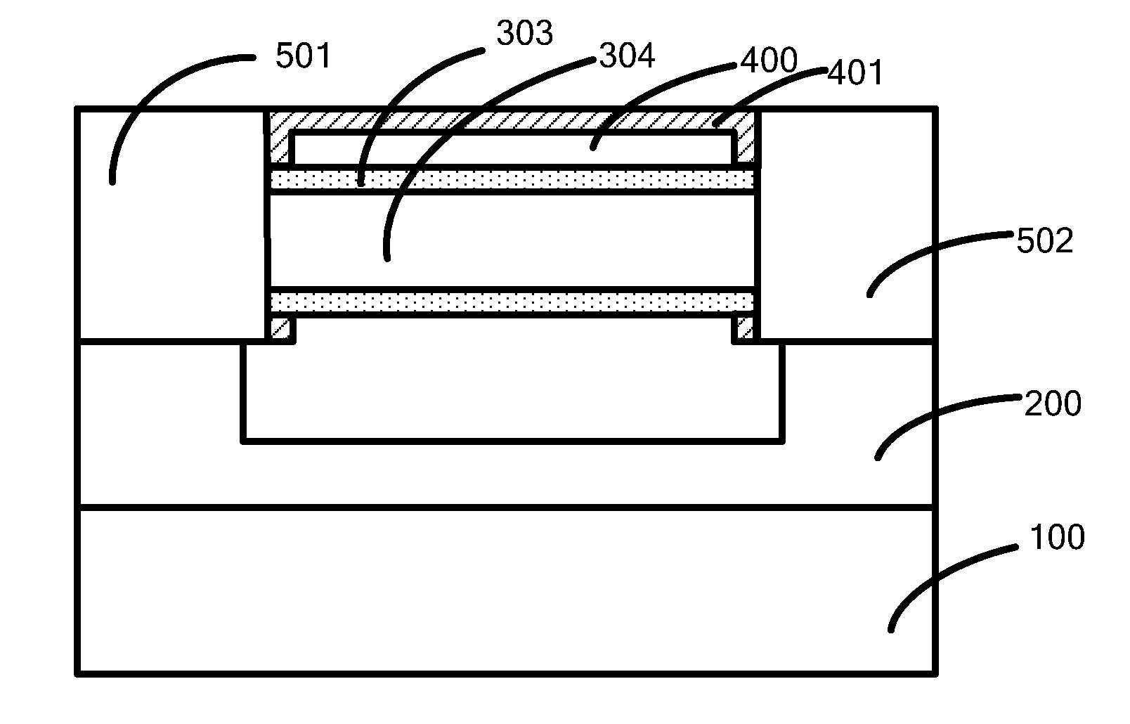
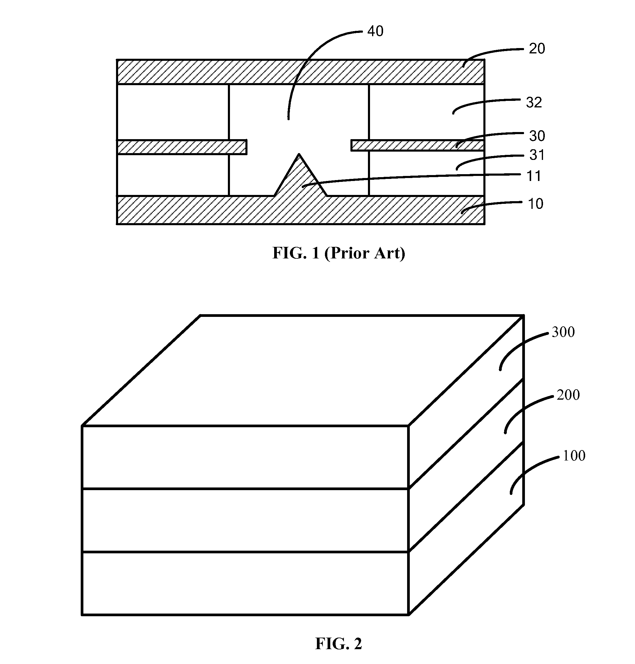
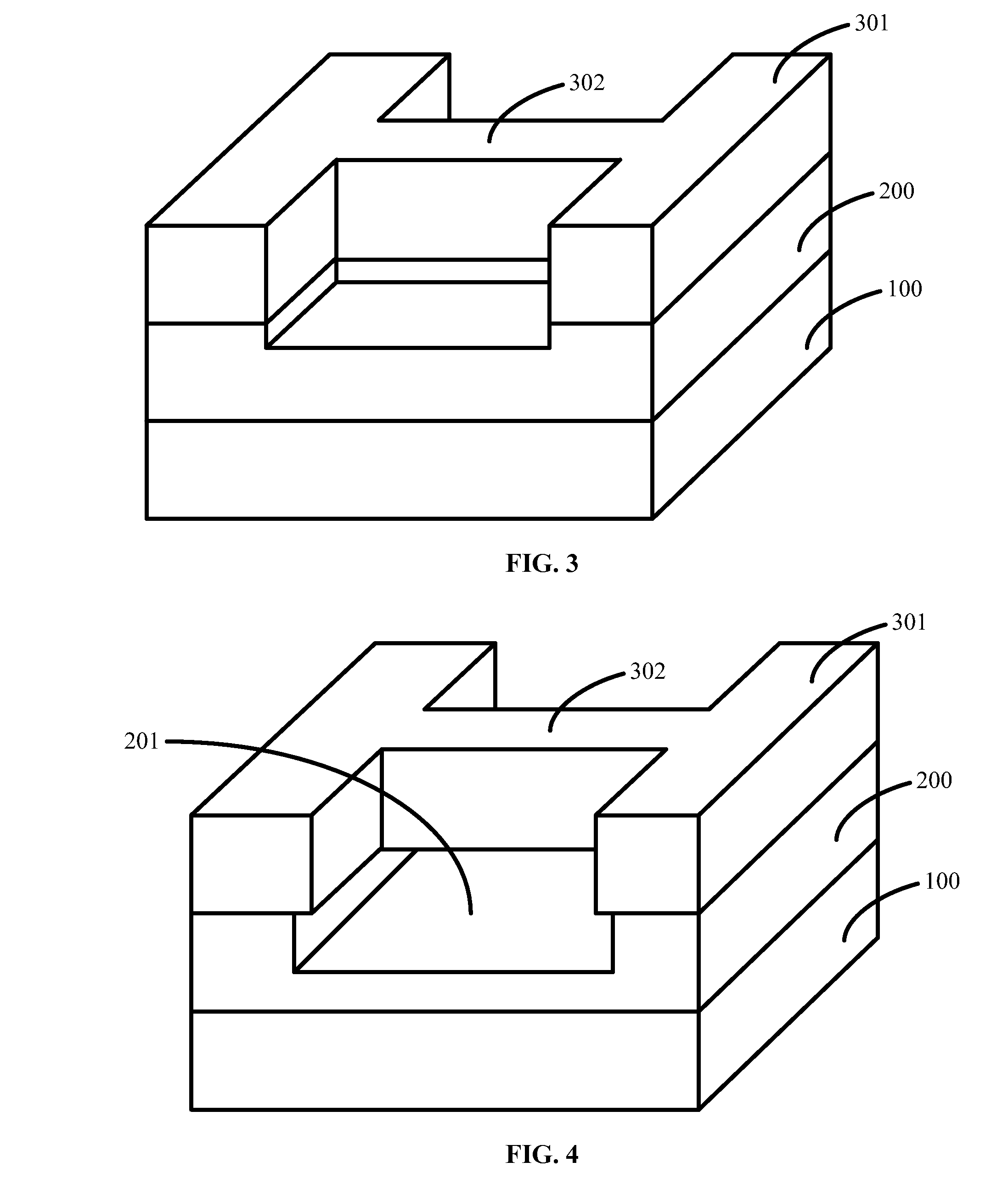
[0016]Reference will now be made in detail to exemplary embodiments of the invention, which are illustrated in the accompanying drawings. Wherever possible, the same reference numbers will be used throughout the drawings to refer to the same or like parts.

[0017]A vacuum tube fabricated by an existing technique may be difficult to integrate with existing integrated circuits (ICs), and the fabrication may be difficult as well. With the shrinkage of the vacuum tube, it may be more difficult to fabricate. Further, because a circular cone may be used as an emitter in the existing vacuum tube, the electric field near to the emitter may be relatively strong. It may be easy for electrons to escape, but the surface of the emitter may be damaged by the high energy discharge generated be the relatively strong electric field, and the performance of the vacuum tube may be reduced. A nano field-effect vacuum tube may be used to overcome such difficulties.

[0018]FIG. 17 illustrates an exemplary fab...


PUM


Abstract

A method is provided for fabricating a nano field-effect vacuum tube. The method includes providing a substrate having an insulating layer and a sacrificial layer; and forming a sacrificial line, a source sacrificial layer and a drain sacrificial layer. The method also includes forming a trench in the insulating layer; and forming a dielectric layer on the surface of the sacrificial line. Further, the method includes forming a metal layer on the dielectric layer to fill up the trench, cover the sacrificial line and expose the source sacrificial layer and the drain sacrificial layer; and removing the source sacrificial layer and the drain sacrificial layer. Further, the method also includes removing the sacrificial line to form a through channel; forming an isolation layer on the metal layer; and forming a source region and a drain region on the insulating layer at both ends of the metal layer.

Description

CROSS-REFERENCES TO RELATED APPLICATIONS[0001]This application claims the priority of Chinese patent application No. 201310170430.3, filed on May 9, 2013, the entirety of which is incorporated herein by reference.FIELD OF THE INVENTION[0002]The present invention generally relates to the field of semiconductor technology and, more particularly, relates to nano field-effect vacuum tubes and fabrication techniques thereof.BACKGROUND[0003]Vacuum tubes may be the earliest electrical signal amplifiers. Vacuum tubes may be used to switch or to modulate electrical signals. They had been used in electronic devices such as televisions, radios, and loudspeakers, etc., for many decades. Nowadays, vacuum tubes are still used as audio power amplifiers in niche applications such as premier sound systems because of the low noise and high stability constants. Vacuum tubes may often be fabricated by mechanical machining processes and used as discrete components, and it may be not easy to integrate va...

Claims


Application Information

Patent Timeline
IPC IPC(8): H01L29/26H01L29/78H01L29/10H01L29/66
CPCH01L29/26B82Y99/00H01L29/1033H01L29/66969H01L29/78H01L29/0665H01L29/66477B82Y40/00H01J21/10H01L29/42392H01L29/78696H01L29/0669H01L29/775
Inventor XIAO, DEYUAN
Owner SEMICON MFG INT (SHANGHAI) CORP
Why Eureka
Try Eureka