Scanning signal line drive circuit and display device equipped with same

Active Publication Date: 2014-11-20
SHARP KK
View PDF5 Cites 12 Cited by
  • Summary
  • Abstract
  • Description
  • Claims
  • Application Information

AI Technical Summary

Benefits of technology

The invention allows for a compact scanning signal line drive circuit with reduced area, which can be mounted on a display panel, resulting in a smaller display panel. The invention also simplifies the selection circuit and drives odd and even scanning signals individually of each other with a simple control signal. The shift register is configured by switching elements and bistable circuits, resulting in circuit simplification and reduced circuit area. The bistable circuits can be configured in a simple manner, and a simple control signal can be used to control the selection circuit, resulting in a reduced circuit area. The invention also allows for the use of simple circuits (such as AND circuits) as logic circuits, resulting in a reduced circuit area.

Problems solved by technology

However, this drive scheme is subject to display defects, such as flicker, upon display, and therefore, in the drive schemes employed in recent years, the polarity of an applied voltage is inverted every horizontal scanning signal line and also every frame (a so-called “line inversion drive scheme”) or the polarity of an applied voltage is inverted every two vertically / horizontally adjacent pixels and also every frame (a so-called “dot inversion drive scheme”).
However, in such a dot inversion drive scheme where a direct-current voltage is applied to the common electrode, the polarity of a video signal to be applied to the liquid crystal panel is switched between predetermined voltages respectively above and below the potential of the common electrode, and therefore, the voltage swing of a video signal outputted by a liquid crystal panel driver is large, so that a specialized power supply configuration is required and power consumption tends to be high.

Method used


Image

  • Scanning signal line drive circuit and display device equipped with same
  • Scanning signal line drive circuit and display device equipped with same
  • Scanning signal line drive circuit and display device equipped with same

Examples


first embodiment

1. First Embodiment

1.1 Overall Configuration and Operation

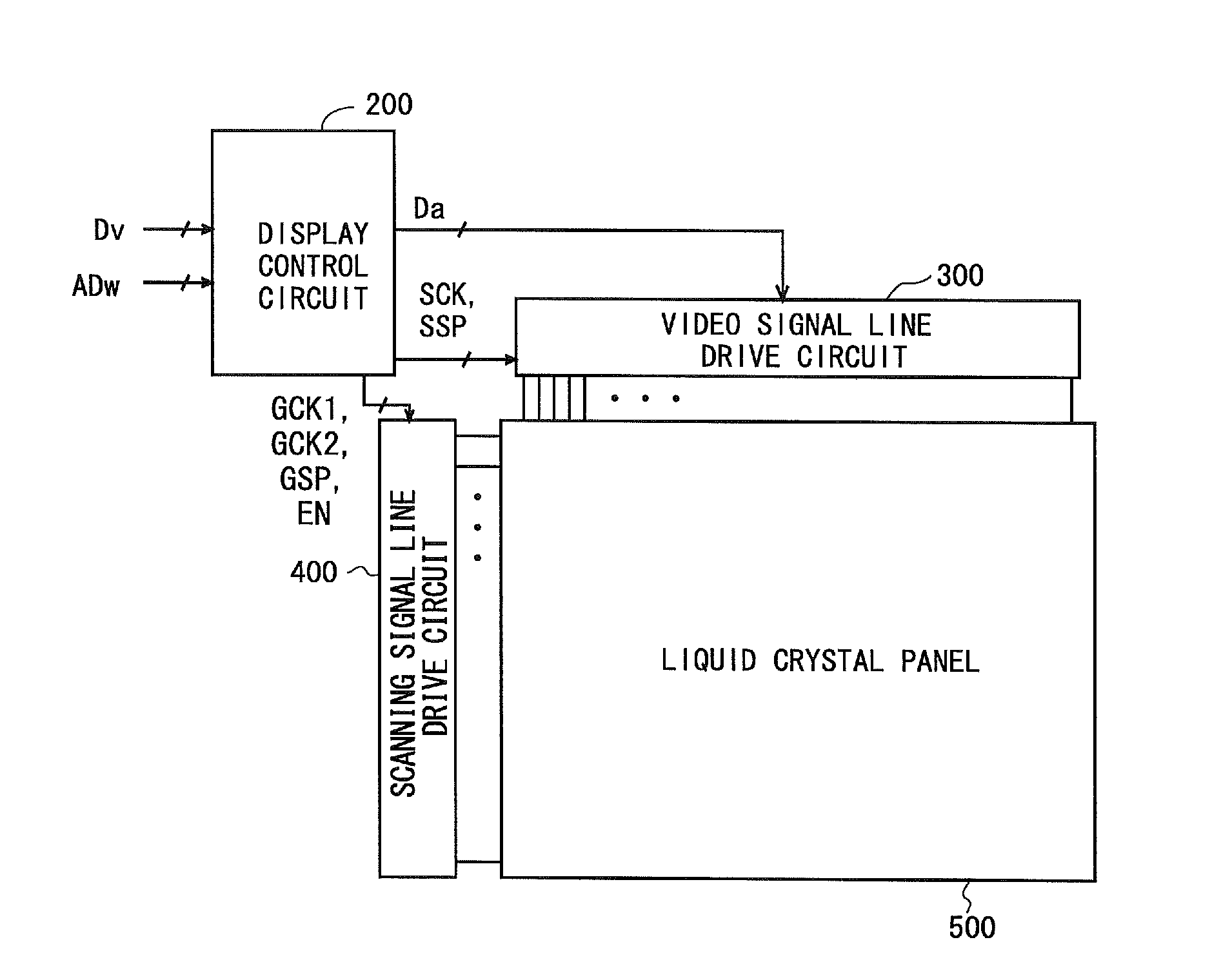
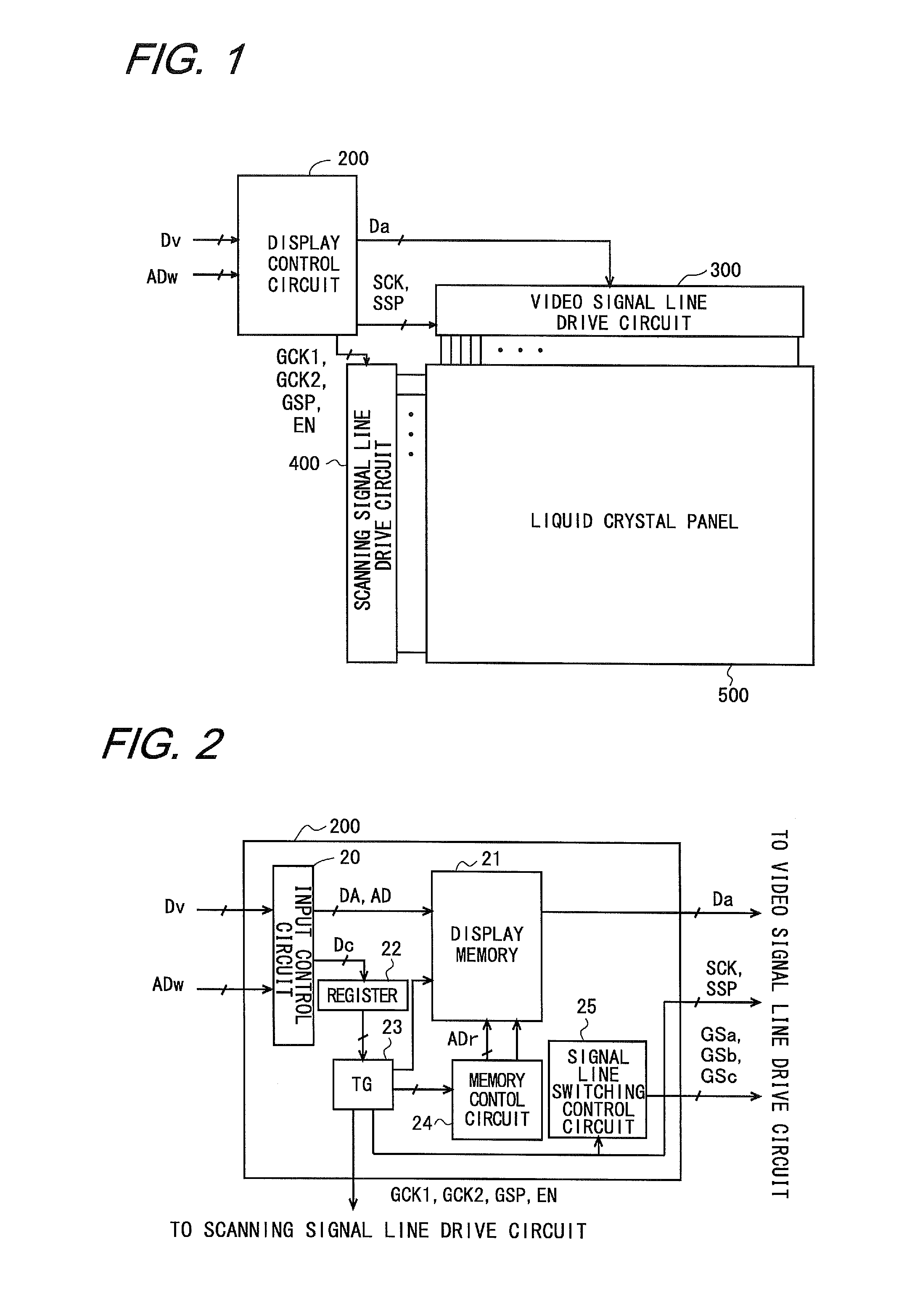
[0043]FIG. 1 is a block diagram illustrating the configuration of a liquid crystal display device according to an embodiment of the present invention. This liquid crystal display device includes a display control circuit 200, a video signal line drive circuit (also referred to as a “source driver circuit” or a “column-electrode drive circuit”) 300, a scanning signal line drive circuit (also referred to as a “gate driver circuit” or a “row-electrode drive circuit”) 400, and an active-matrix liquid crystal panel 500.

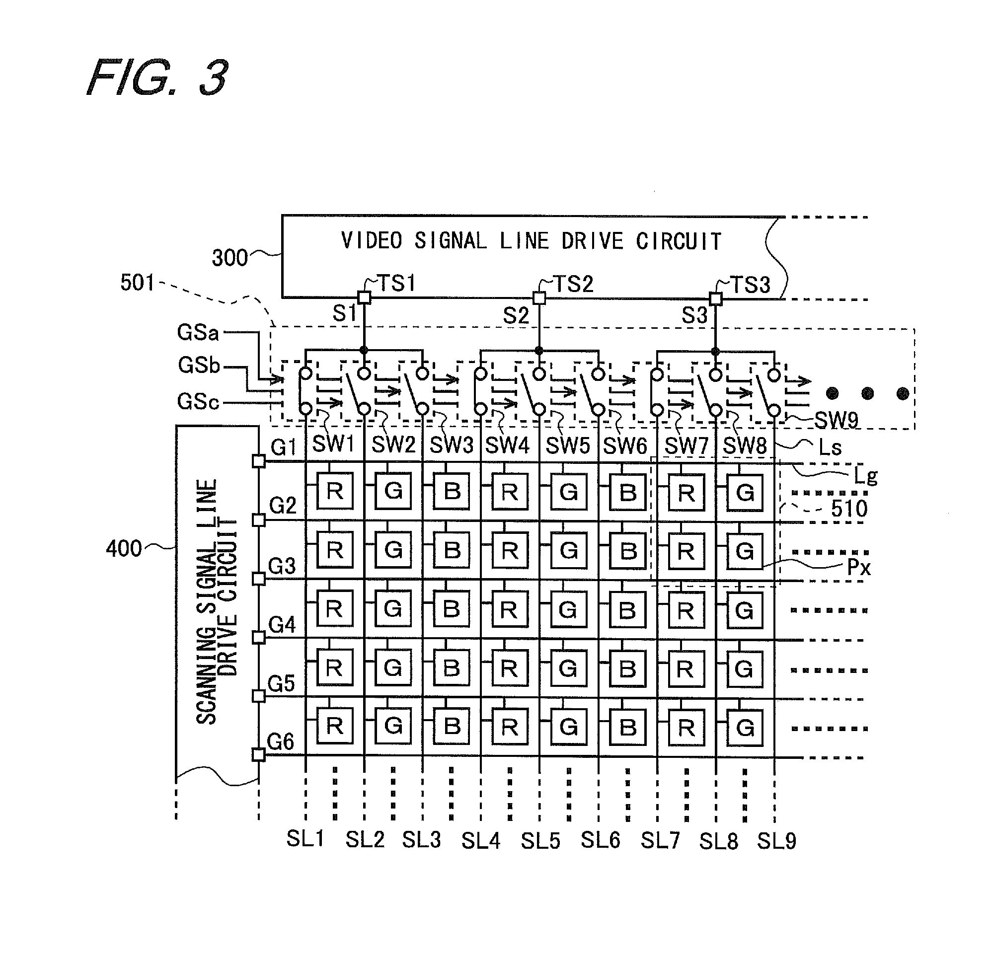
[0044]The liquid crystal panel 500, which serves as a display portion of the liquid crystal display device, includes a plurality of scanning signal lines (row electrodes), which correspond to respective horizontal scanning lines in an image represented by image data Dv received from a CPU or suchlike in an external computer, a plurality of video signal lines (column electrodes), which cross each of the scanning sign...

second embodiment

2. Second Embodiment

2.1 Overall Configuration and Operation

[0091]Because the configuration of a liquid crystal display device according to a second embodiment of the present invention is similar to the configuration shown in FIG. 1 and the configuration and other details of the liquid crystal panel 500 are similar to those shown in, for example, FIG. 3, the same components are denoted by the same reference characters and any detailed descriptions thereof will be omitted. However, the present embodiment is different in terms of the logic circuit configuration that functions as a selection circuit included in the scanning signal line drive circuit 400. Detailed descriptions will be given below with reference to FIG. 11.

2.2 Configuration and Operation of the Scanning Signal Line Drive Circuit

[0092]FIG. 11 is a block diagram illustrating in detail the configuration of the scanning signal line drive circuit in the present embodiment. As with the scanning signal line drive circuit 400 in ...

third embodiment

3. Third Embodiment

3.1 Overall Configuration and Operation

[0098]Because the configuration of a liquid crystal display device according to a third embodiment of the present invention is similar to the configuration shown in FIG. 1, and the configuration and other details of the liquid crystal panel 500 are similar to those shown in, for example, FIG. 3, the same components are denoted by the same reference characters and any detailed descriptions thereof will be omitted. In addition, the configuration of the scanning signal line drive circuit is similar to that in the first or second embodiment, and therefore, any description thereof will be omitted.

[0099]However, the present embodiment employs a 1-dot inversion drive scheme as shown in FIG. 13, rather than a line inversion drive scheme or a 3-dot inversion drive scheme as employed in the first (or second) embodiment or a variant thereof.

[0100]FIG. 13 is a diagram describing such a 1-dot inversion drive operation. As shown in FIG. 13...


PUM


Abstract

This liquid crystal display device allows outputs from RS-FF circuits (401 to 409) and switch circuits (411 to 419), which function as a shift register, to be provided as scanning signals that are selectively activated during odd and even scanning line selection periods, by simply changing the potential of an enable signal (EN) (i.e., by simply providing an EN signal line), which achieves interlacing drive that allows a reduction in the number of polarity inversions, thereby making it possible to reduce power consumption and a wiring area for control lines and achieve simple control which allows circuit simplification, resulting in a reduced frame area and a display panel which is compact as a whole.

Description

TECHNICAL FIELD[0001]The present invention relates to active-matrix display devices, more specifically to a scanning signal line drive circuit in an active-matrix liquid crystal display device.BACKGROUND ART[0002]In general liquid crystal display devices, polarity inversion drive is performed in order to suppress liquid crystal deterioration. A known polarity inversion drive scheme is a scheme (frame inversion drive scheme) in which the polarity of a voltage applied to the liquid crystal is inverted every frame. However, this drive scheme is subject to display defects, such as flicker, upon display, and therefore, in the drive schemes employed in recent years, the polarity of an applied voltage is inverted every horizontal scanning signal line and also every frame (a so-called “line inversion drive scheme”) or the polarity of an applied voltage is inverted every two vertically / horizontally adjacent pixels and also every frame (a so-called “dot inversion drive scheme”).[0003]The dot ...

Claims


Application Information

Patent Timeline
IPC IPC(8): G09G3/36G02F1/1362
CPCG02F1/1362G09G3/3648G09G3/3614G09G3/3677G09G2310/0224G09G2310/0286
Inventor YOKONUMA, SHINSUKEWASHIO, HAJIME
Owner SHARP KK
Why Eureka
Try Eureka