Photoconductive device with plasmonic electrodes

a plasmonic electrode and photoconductive technology, applied in the field of photoconductive devices, can solve the problems of low power, inefficiency, thermal breakdown, high cost, etc., and achieve the effect of improving the quantum efficiency of the photoconductive devi

Active Publication Date: 2014-11-27
RGT UNIV OF CALIFORNIA
View PDF2 Cites 51 Cited by
  • Summary
  • Abstract
  • Description
  • Claims
  • Application Information

AI Technical Summary

Benefits of technology

[0005]According to one aspect, there is provided a photoconductive device for emitting or detecting terahertz (THz) radiation. The photoconductive device may comprise: a semiconductor substrate; an antenna assembly fabricated on the semiconductor substrate; and a photoconductor assembly fabricated on the semiconduct

Problems solved by technology

Although there is much potential for the commercial use of THz-TDS systems, their use thus far has been somewhat hindered by certain drawbacks, such as their low power, inefficiency, high cost, thermal breakdown, complexity, and the bulky nature of existing terahertz sources.
For example, most existing terahertz (THz) spectrometers are not broadly used for military and commercial chemical detection and/or characterization purposes.
This is mainly due to the drawbacks mentioned above which can hinder the practical feasibility of such systems, particularly in portable syste

Method used


Image

  • Photoconductive device with plasmonic electrodes
  • Photoconductive device with plasmonic electrodes
  • Photoconductive device with plasmonic electrodes

Examples


Embodiment Construction

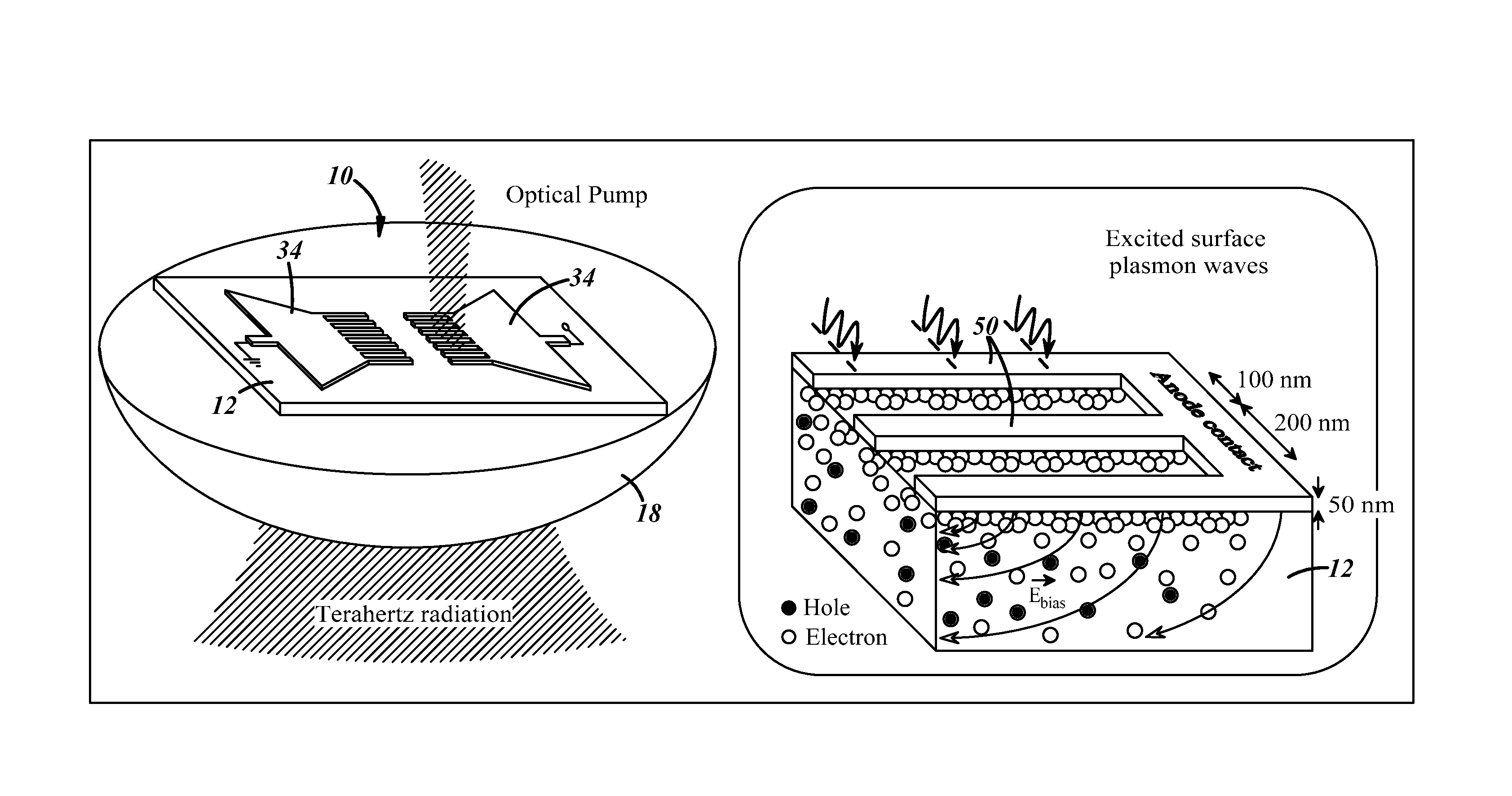
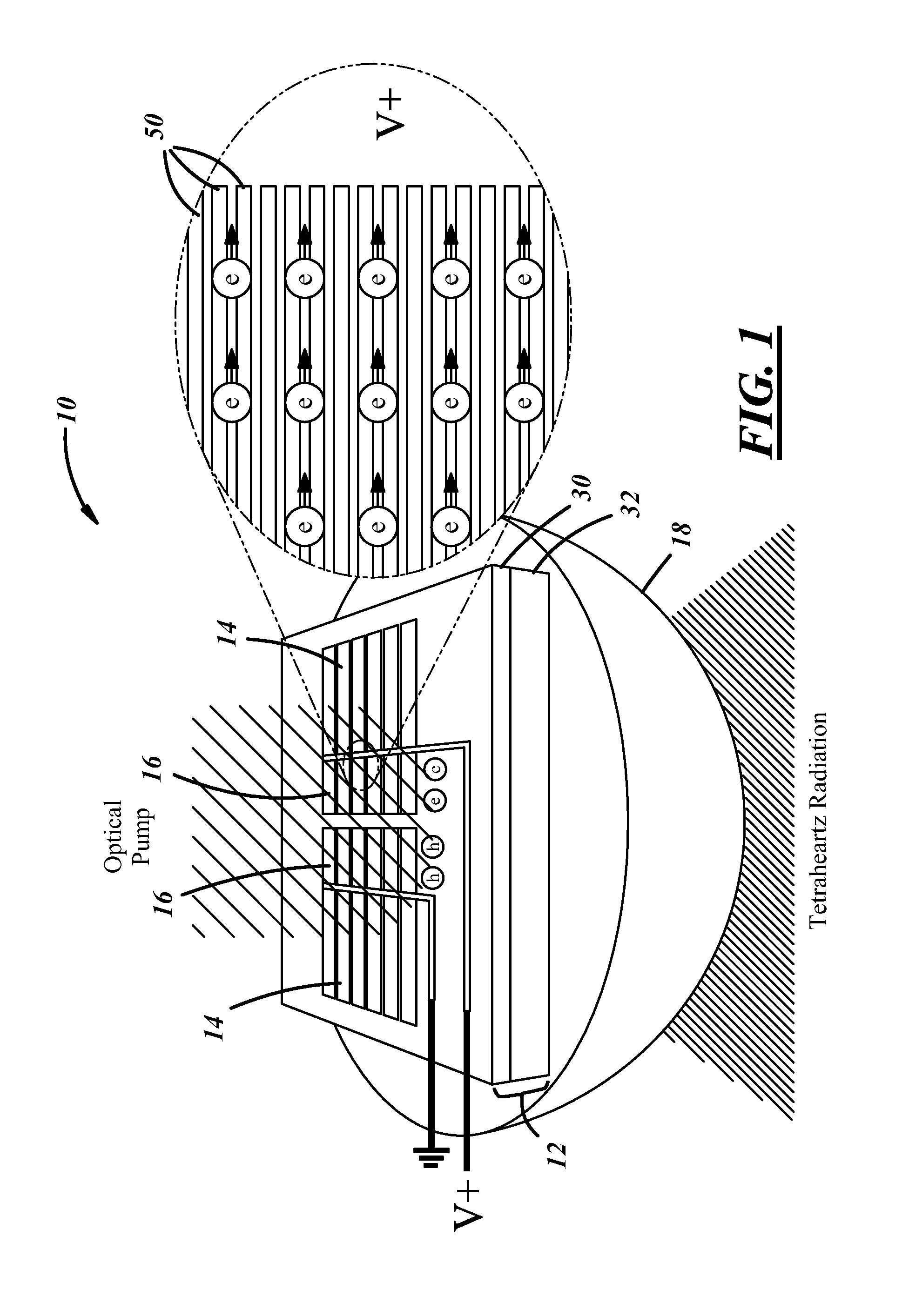
[0019]The photoconductive devices described herein address some of the performance limitations of existing photoconductive devices. According to an exemplary embodiment, the photoconductive device may be a high-performance plasmonic-distributed photoconductive terahertz source that is pumped at telecom pump wavelengths (e.g., 1.0-1.6 μm) for which high power, narrow linewidth, frequency tunable, compact and cost-efficient optical sources are available. A photoconductor assembly having a number of distributed plasmonic contact electrodes may significantly enhance the pump coupling efficiency, while enabling ultra high-speed collection of photo-generated carriers and mitigating the carrier screening effect and thermal breakdown limitations that can occur while operating at high pump power levels. This, in turn, may enable terahertz power levels that are significantly higher than those currently available. According to one exemplary implementation, the photoconductive device is a frequ...


PUM


Abstract

A photoconductive device that includes a semiconductor substrate, an antenna assembly, and a photoconductive assembly with one or more plasmonic contact electrodes. The photoconductive assembly can be provided with plasmonic contact electrodes that are arranged on the semiconductor substrate in a manner that improves the quantum efficiency of the photoconductive device by plasmonically enhancing the pump absorption into the photo-absorbing regions of semiconductor substrate. In one exemplary embodiment, the photoconductive device is arranged as a photoconductive source and is pumped at telecom pump wavelengths (e.g., 1.0-1.6 μm) and produces milliwatt-range power levels in the terahertz (THz) frequency range.

Description

STATEMENT OF FEDERALLY-SPONSORED RESEARCH[0001]This invention was made with government support under N66001-10-1-4027 awarded by Navy / SPAWAR, W911NF-12-1-0253 awarded by the Army Research Office, N00014-11-1-0856 awarded by the Office of Naval Research, EECCS1054454 Awarded by the National Science Foundation, N00014-11-1-0096 awarded by the Office of Naval Research. The government has certain rights in the invention.TECHNICAL FIELD[0002]This invention relates generally to photoconductive devices and, more particularly, to photoconductive devices that emit or detect terahertz (THz) waves using plasmonic electrodes for improved quantum efficiency.BACKGROUND OF THE INVENTION[0003]Terahertz (THz) waves possess a number of unique capabilities and properties, including ones that make them useful for chemical identification, material characterization, biological sensing, and medical imaging, to cite a few examples. Terahertz Time Domain Spectroscopy (THz-TDS) is a spectroscopic technique t...

Claims


Application Information

Patent Timeline
IPC IPC(8): G01J3/10H01L33/38H01L33/04H01L31/0224H01L31/0352
CPCG01J3/108H01L31/0224H01L33/38H01L33/04H01L31/035209H01L31/09H01L31/02327
Inventor JARRAHI, MONABERRY, CHRISTOPHER W.WANG, NINGYANG, SHANG-HUAHASHEMI, MOHAMMED REZA MAHMOODI
Owner RGT UNIV OF CALIFORNIA
Why Eureka
Try Eureka