

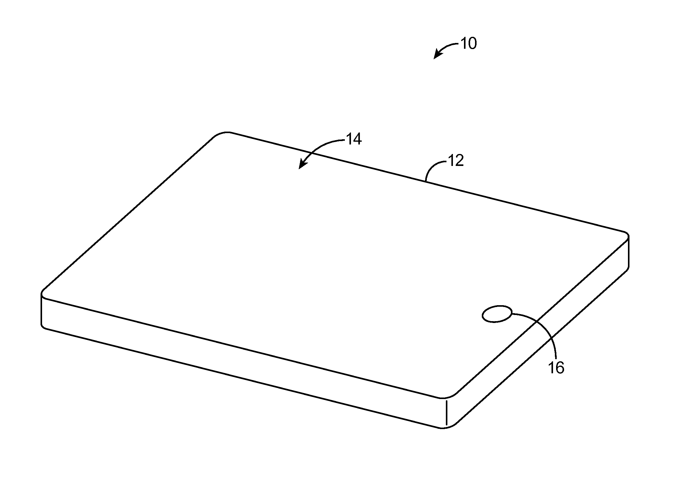
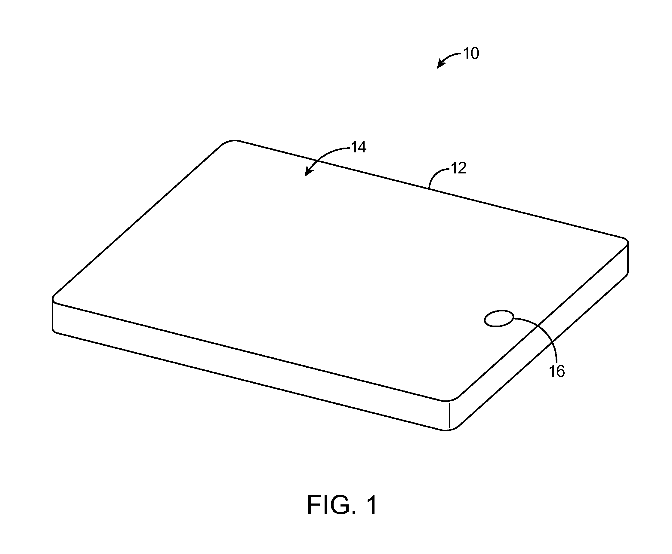
Flexible Printed Circuit Cables With Slits
a printed circuit cable and flexible technology, applied in the field of flexible printed circuit cables for electronic devices, can solve the problems of other potential failures, excessive stress on the flexible printed circuit cable, and difficulty in using this type of cabl
- Summary
- Abstract
- Description
- Claims
- Application Information
AI Technical Summary
Benefits of technology
Problems solved by technology
Method used
Image

Examples
Embodiment Construction
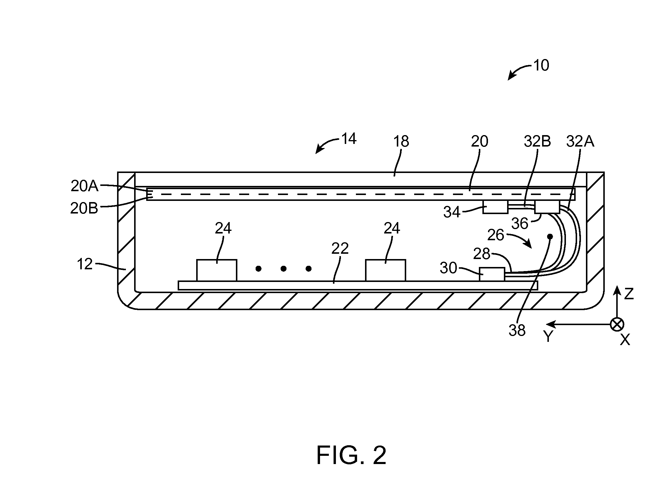
[0023]Flexible printed circuits are formed from layers of flexible polymer or other dielectric and patterned metal traces. Substrates that may be used in forming flexible printed circuits include layers of polyimide and sheets of other flexible polymer materials. Metal traces on flexible printed circuits may be formed from metals such as copper or other traces that can be patterned into signal lines and ground plane structures. Metal flexible printed circuit traces may be patterned using blanket physical vapor deposition followed by photolithographic patterning, by depositing metal lines using ink-jet printing or screen printing techniques, using laser-based processing (e.g., using laser light to selectively activate substrate regions followed by electroplating to grow metal on the activated regions), or by using other suitable patterning techniques.
[0024]The metal traces on flexible printed circuits can be used to form serial and parallel digital data signal paths and analog signal...
PUM
 Abstract
Description
Claims
Application Information