Integrated circuit
a technology of integrated circuits and integrated circuits, applied in pulse generators, pulse techniques, instruments, etc., can solve the problems of inability to use the operation frequency of the disclosed mtj/cmos hybrid integrated circuit, inability to write data at high speed to a memory device having long data retention time, and inability to achieve the effect of reducing power consumption, reducing power consumption, and improving the reversal probability of memory elements
- Summary
- Abstract
- Description
- Claims
- Application Information
AI Technical Summary
Benefits of technology
Problems solved by technology
Method used
Image

Examples
first embodiment
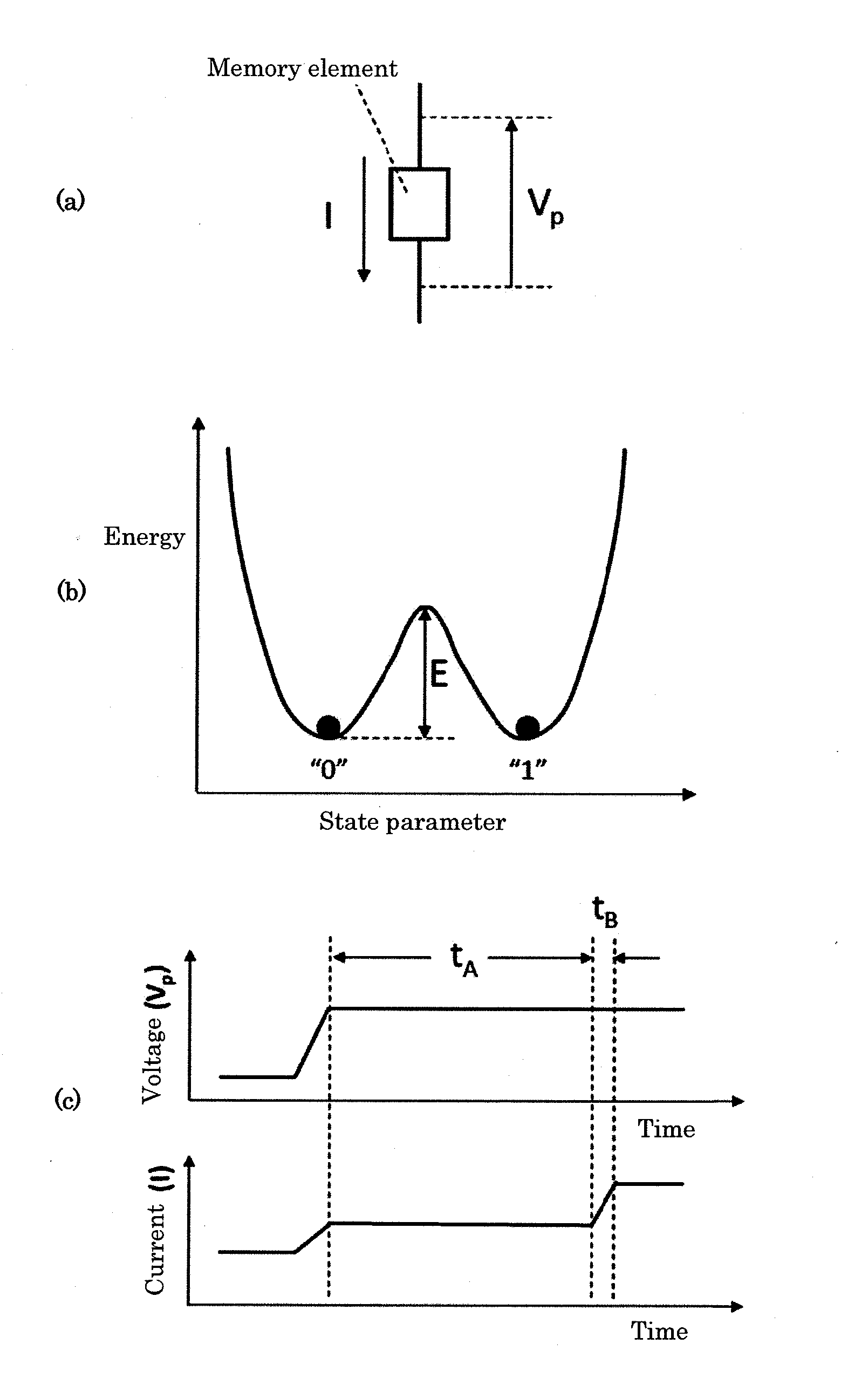
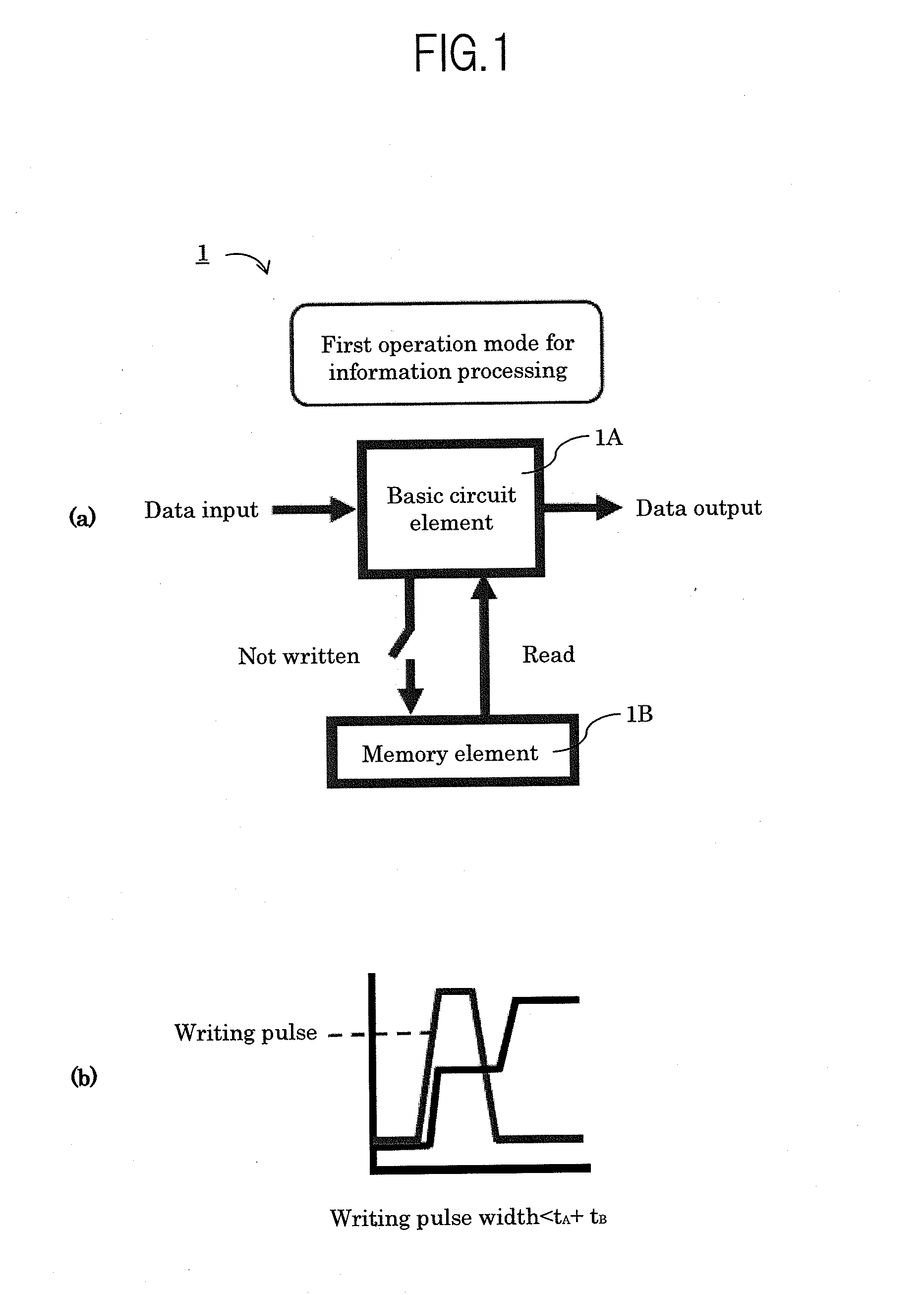
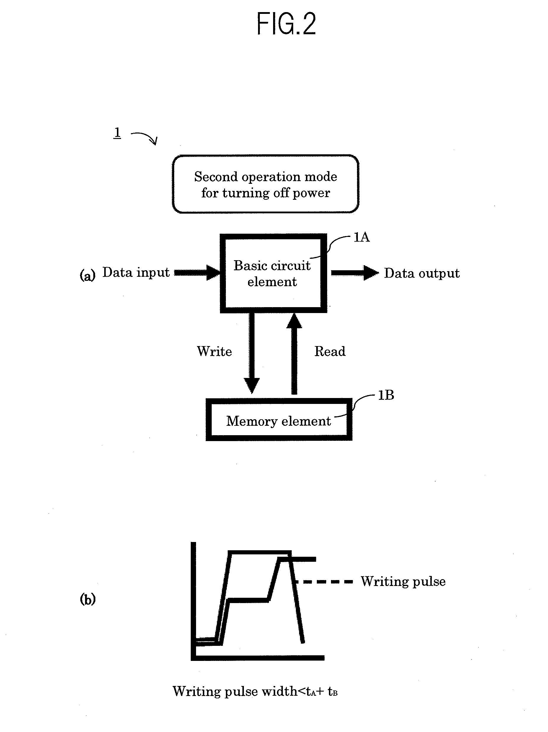
[0293]FIG. 1 is a diagram describing a first operation mode where information processing is performed in the basic structure of the integrated circuit 1 of the present invention, where (a) is a block diagram, and (b) is a time chart showing a write pulse. FIG. 2 is a diagram describing a second operation mode for turning off power in the basic structure of the integrated circuit 1 of the present invention, where (a) is a block diagram, and (b) is a time charts showing a write pulse. FIG. 3 is a time chart showing the first to the fourth modes of the integrated circuit 1 of the present invention.
[0294]As shown in FIG. 1, the integrated circuit 1 of the present invention includes: a basic circuit element 1A; and a memory element 1B capable of storing volatile data of the basic circuit element 1A. The basic circuit element 1A is a circuit for processing or retaining volatile data, and includes: logic circuits such as a latch circuit, D-latch circuit, flip-flop circuit (also called FF c...
second embodiment
Latch
[0330]Next, a latch will be described as a second embodiment.
[0331]FIG. 17 is a circuit diagram showing a latch as the basic structure of the second embodiment of the integrated circuit 1C of the present invention. FIG. 18 is a diagram of a control circuit 38 for generating input control signal WCK used in FIG. 17.
[0332]As shown in FIG. 17, the integrated circuit 1C of the present invention includes: a first latch 10; the spin-injection-type MTJ devices 15, 16 connected to the first latch 10; and a second latch 20 connected to the spin-injection-type MTJ devices 15, 16. With the spin-injection-type MTJ devices 15, 16, the data is written at an operation frequency lower than that of the first latch 10 and / or the second latch 20. The first latch 10 is also called a lower latch, and the second latch 20 is also called an upper latch. In the following description, the spin-injection-type MTJ device is simply called an MTJ device.
[0333]The first latch 10 includes: a first circuit 2; ...
modification example 9
of the Second Embodiment
[0412]FIG. 38 is a circuit diagram of the modification example 9 of an integrated circuit 50 according to the second embodiment of the present invention. FIG. 39 is a time chart showing the operation of the integrated circuit 50 as shown in FIG. 38.
[0413]As shown in FIG. 38, according to the integrated circuit 50 of the modification example 9, n-type MOSFETs 25, 26 are further connected as the load transistors to n-type MOSFET's 2a, 4a in the first latch 10 of the integrated circuit 40 of the second embodiment as shown in FIG. 30.
[0414]In particular, the drain of the left load transistor 25 is connected to the drain of the n-type MOSFET 2a, the source of the load transistor 25 is grounded, and the PWON signal is applied to the gate of the load transistor 25. The drain of the right load transistor 26 is connected to the drain of the n-type MOSFET 4a, the source of the load transistor is grounded, and the PWON signal is applied to the gate of the load transisto...
PUM
 Abstract
Description
Claims
Application Information
 - R&D
- Intellectual Property
- Life Sciences
- Materials
- Tech Scout
- Unparalleled Data Quality
- Higher Quality Content
- 60% Fewer Hallucinations
Browse by: Latest US Patents, China's latest patents, Technical Efficacy Thesaurus, Application Domain, Technology Topic, Popular Technical Reports.
© 2025 PatSnap. All rights reserved.Legal|Privacy policy|Modern Slavery Act Transparency Statement|Sitemap|About US| Contact US: help@patsnap.com