Pixel circuit and display device
a display device and circuit technology, applied in static indicating devices, instruments, electroluminescent light sources, etc., can solve the problems of increasing the resistance of the cathode electrode, the difficulty of forming an organic film of good quality on the cathode electrode, etc., to suppress the potential change of the gate electrode, the capacitance of the capacitance element can be sufficiently large, and the leak current of the transistor element is significantly suppressed
- Summary
- Abstract
- Description
- Claims
- Application Information
AI Technical Summary
Benefits of technology
Problems solved by technology
Method used
Image
Examples
first embodiment
[0057]In a first embodiment, there will be described circuit configurations and operations of the display device of the present invention (hereinafter simply referred to as display device) and the pixel circuit of the present invention (hereinafter simply referred to as pixel circuit).
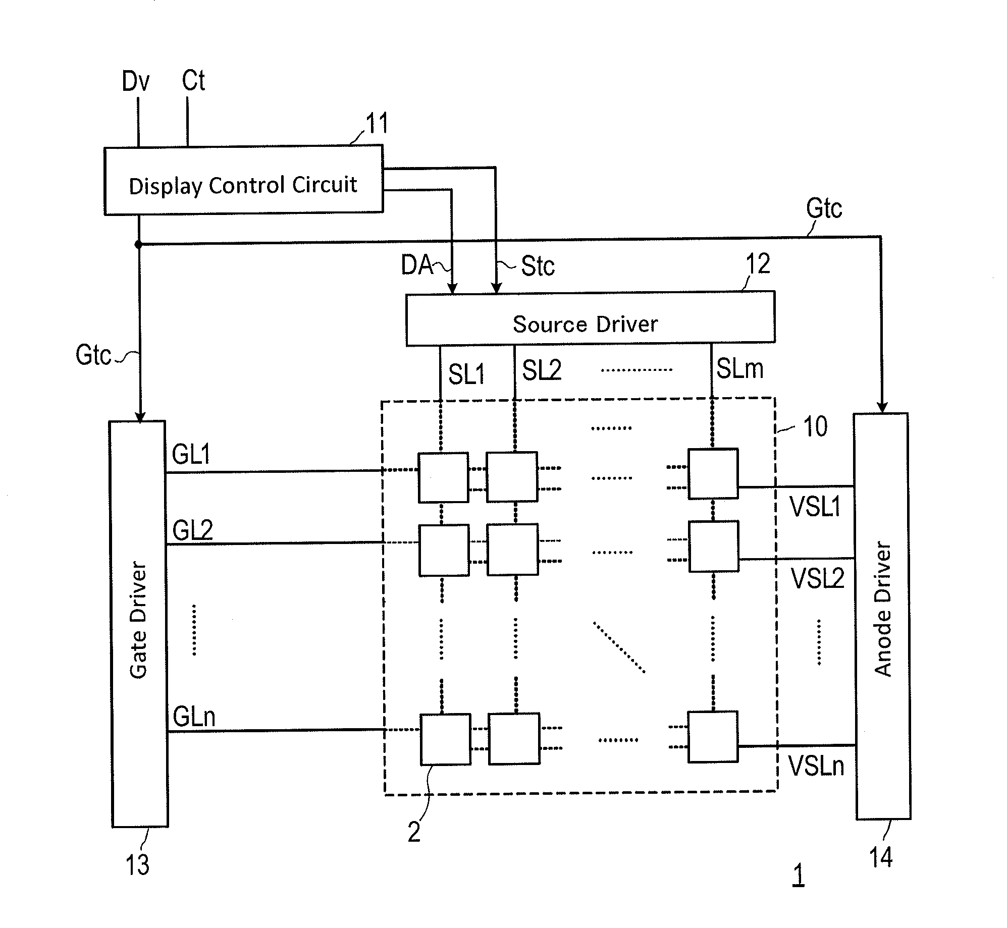
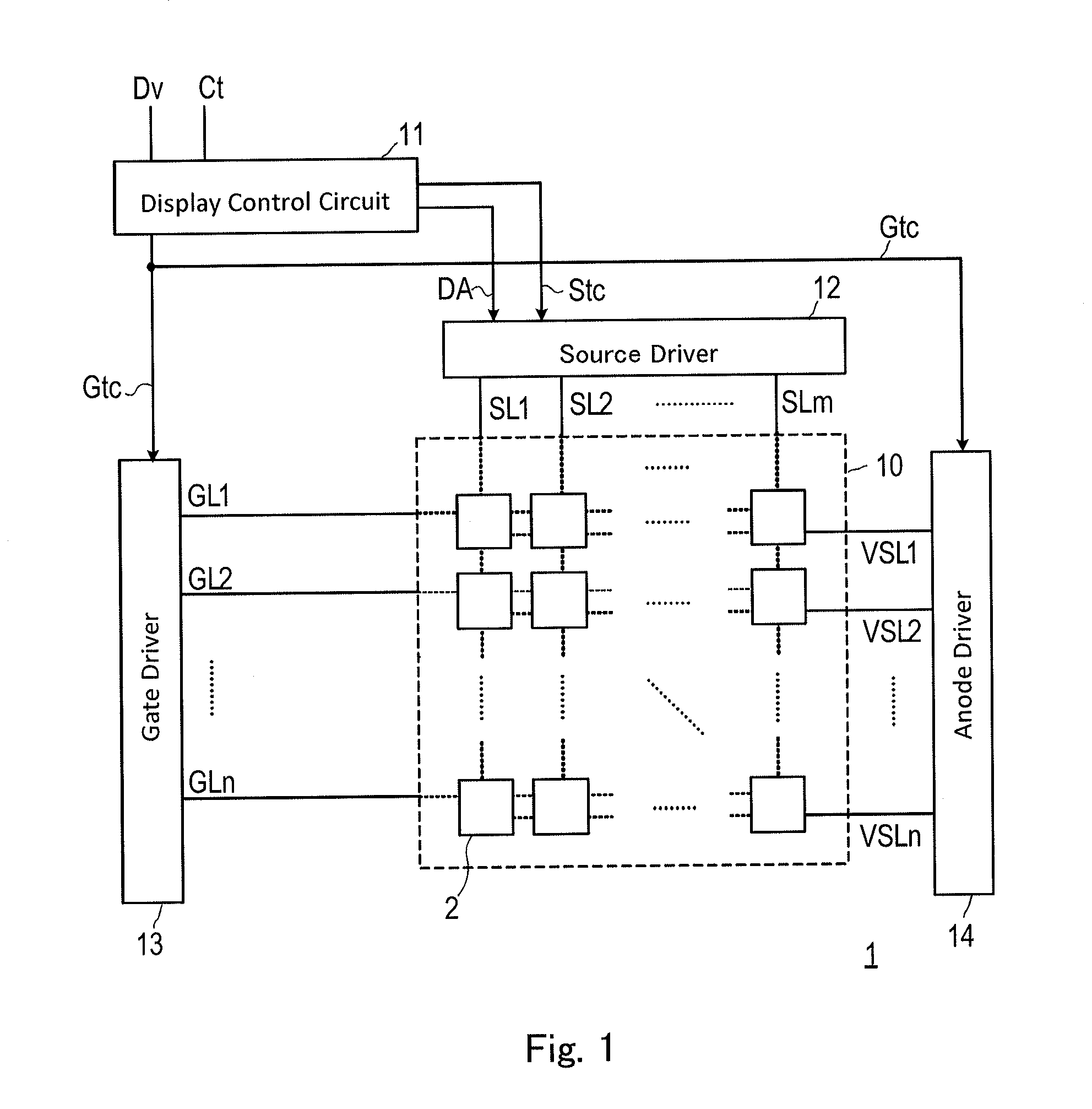
[0058]FIG. 1 shows a schematic configuration of a display device 1. The display device 1 includes a pixel circuit array 10, a display control circuit 11, a source driver 12, a gate driver 13 and an anode driver 14. The pixel circuit array 10 is configured by arranging on an active matrix substrate a plurality of pixel circuits 2 in a row direction and a column direction. It is to be noted that in FIG. 1, the pixel circuits 2 are illustrated by blocks in order to avoid complexity of the drawing.
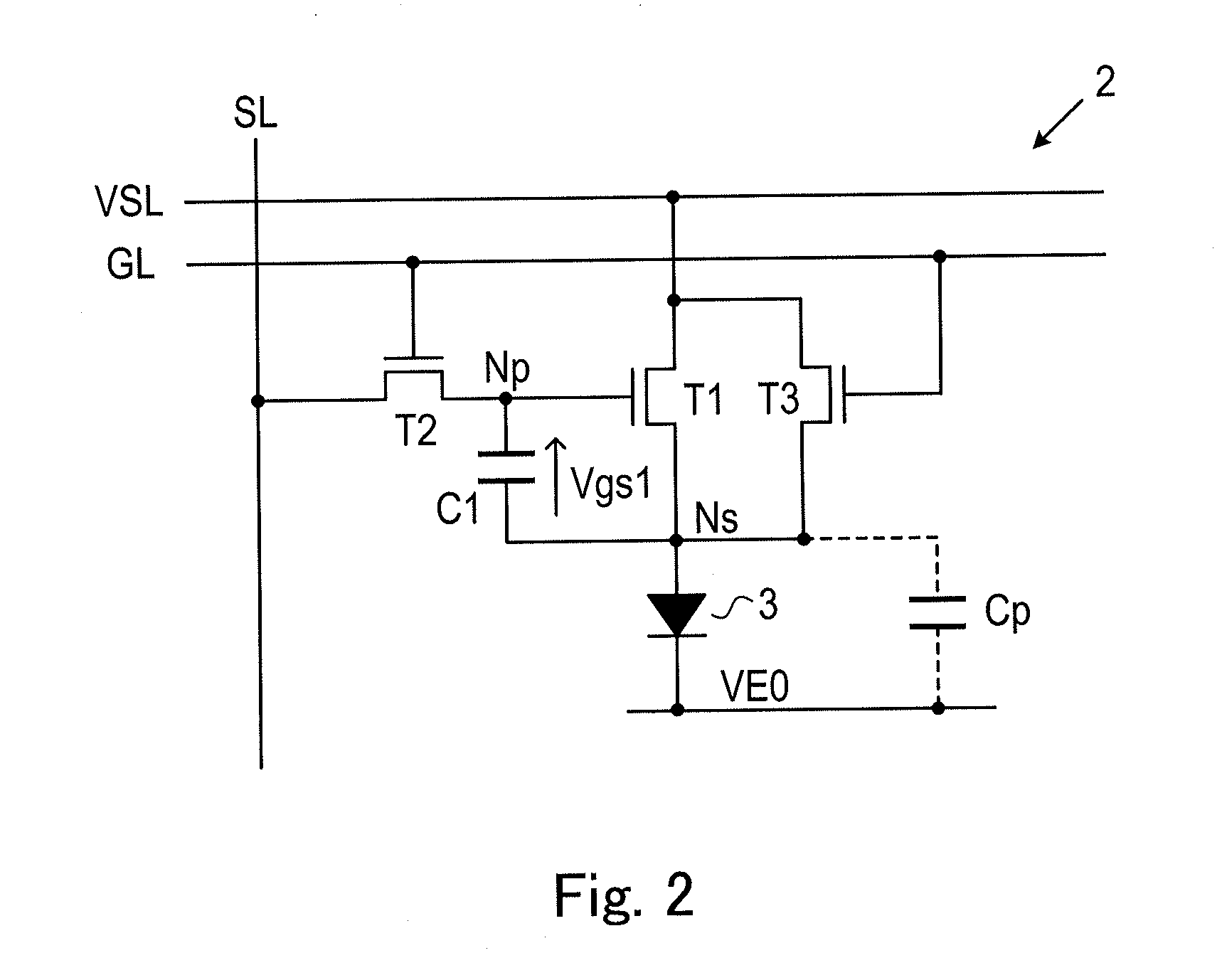
[0059]FIG. 2 shows an equivalent circuit diagram of the pixel circuit 2. As shown in FIG. 2, the pixel circuit 2 is configured including an organic EL element (OLED) 3, a drive transistor T1, a transfer transisto...
second embodiment
[0078]In a second embodiment, a description will be given of a circuit configuration to perform compensation not within the individual pixel circuits 2 but outside the pixel circuit array 10 in a case where the transistor characteristic (threshold voltage, mobility, etc.) of the drive transistor T1 changes due to electric stress that is applied by repeatedly performing the above write operation.
[0079]FIG. 5 shows a schematic configuration of a display device 4 according to the second embodiment. The display device 4 is provided with a monitor circuit 30 and a correction circuit 31 on top of the pixel circuit array 10, the display control circuit 11, the source driver 12, the gate driver 13 and the anode driver 14. The pixel circuit array 10, the display control circuit 11, the source driver 12, the gate driver 13, the anode driver 14, and the pixel circuits 2 constituting the pixel circuit array 10 have the same circuit configuration as that of the display device 1 described in the ...
PUM
 Abstract
Description
Claims
Application Information


