Test circuit and method for semiconductor device

a test circuit and semiconductor technology, applied in semiconductor/solid-state device testing/measurement, semiconductor/solid-state device details, instruments, etc., can solve the problems of difficult to accurately measure the resistance of the tsv, measurement error becomes significant, and measurement accuracy is difficult to achieve. , to achieve the effect of reducing measurement error

Active Publication Date: 2014-12-18
SK HYNIX INC
View PDF10 Cites 8 Cited by
  • Summary
  • Abstract
  • Description
  • Claims
  • Application Information

AI Technical Summary

Benefits of technology

[0009]An embodiment of the present invention is directed to a semiconductor device that may minimize measurement error in testing a Through-Silicon-Via (TSV) of stacked chips after packaging.

Problems solved by technology

Such measurement, however, hardly measures the resistance of the TSV because of noise including resistance due to the distance to the test pad and a transistor involved in the measurement.
Since the resistance of the transistor involved in the measurement is relatively greater than the resistance of the TSV, measurement error becomes significant.
After all, since errors occur from the PVT (Process, Voltage, and Temperature) of the transistor involved in the measurement, it is difficult to accurately measure the resistance of the TSV.

Method used


Image

  • Test circuit and method for semiconductor device
  • Test circuit and method for semiconductor device
  • Test circuit and method for semiconductor device

Examples


Embodiment Construction

[0020]Exemplary embodiments of the present invention will be described below in more detail with reference to the accompanying drawings. The present invention may, however, be embodied in different forms and should not be construed as limited to the embodiments set forth herein. Rather, these embodiments are provided so that this disclosure will be thorough and complete, and will fully convey the scope of the present invention to those skilled in the art. Throughout the disclosure, reference numerals correspond directly to the like numbered parts in the various figures and embodiments of the present invention. It is also noted that in this specification, “connected / coupled” refers to one component not only directly coupling another component but also indirectly coupling another component through an intermediate component. In addition, a singular form may include a plural form as long as it is not specifically mentioned in a sentence.

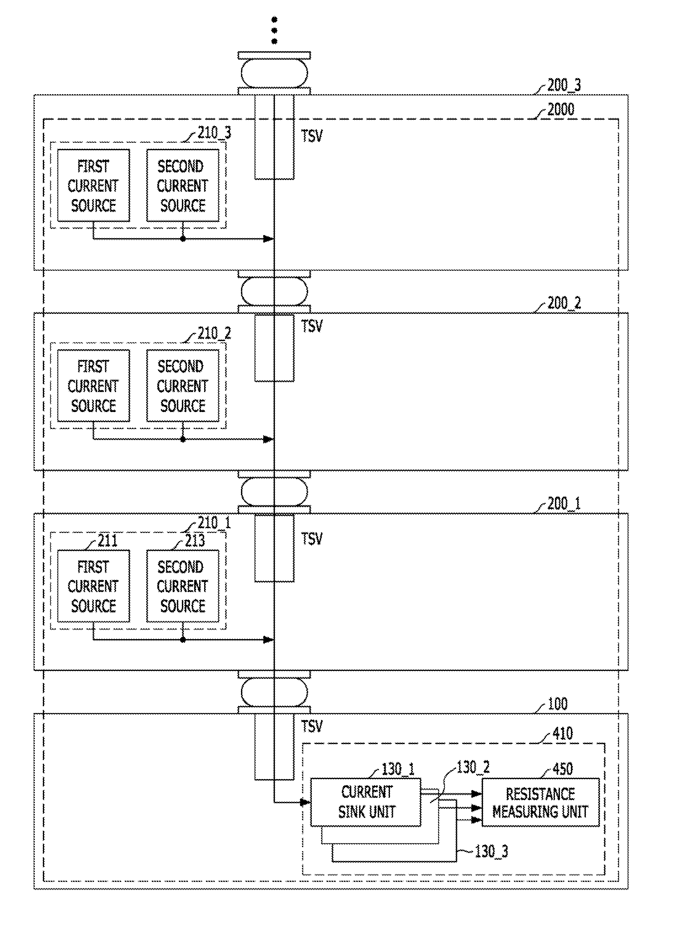
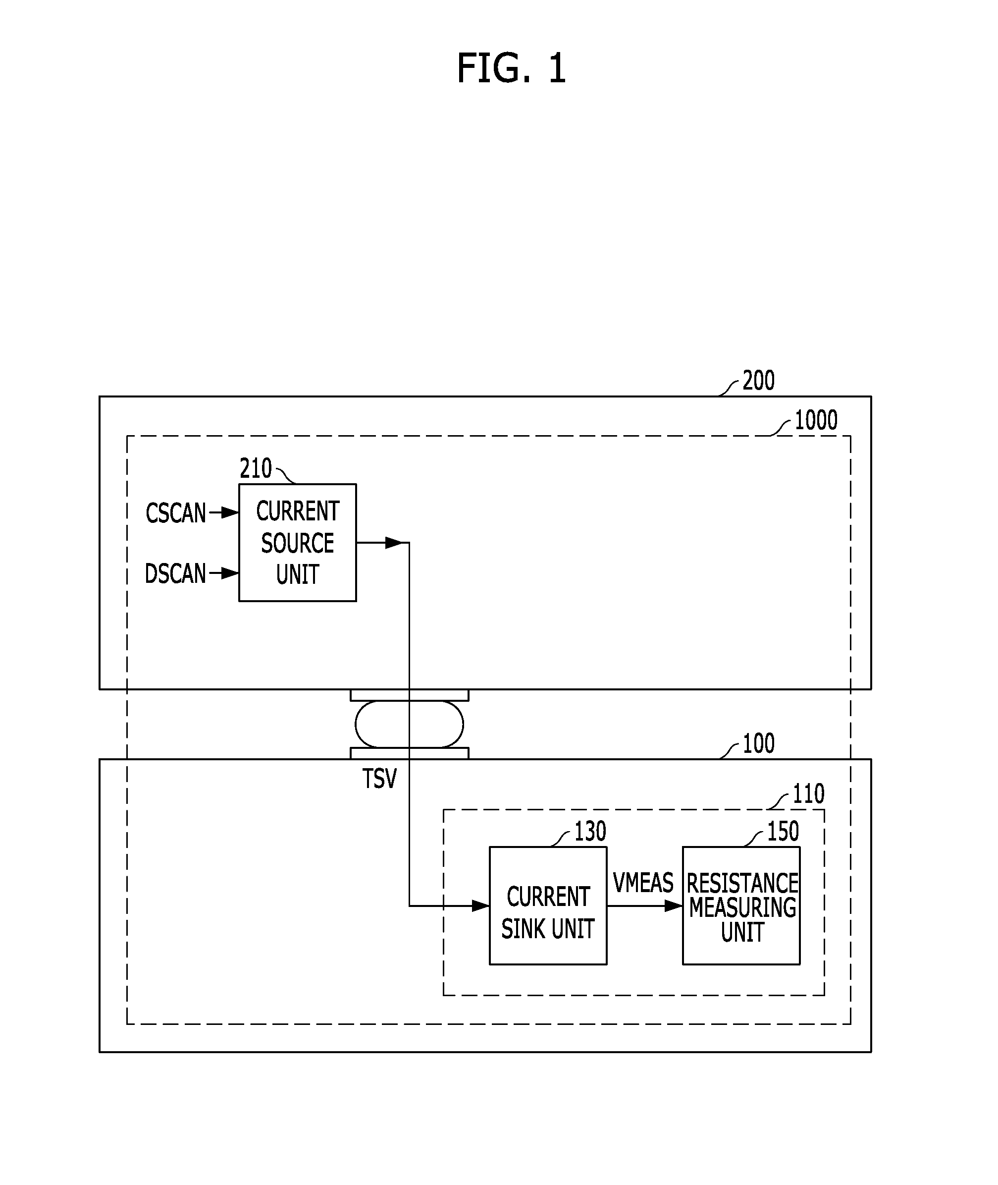
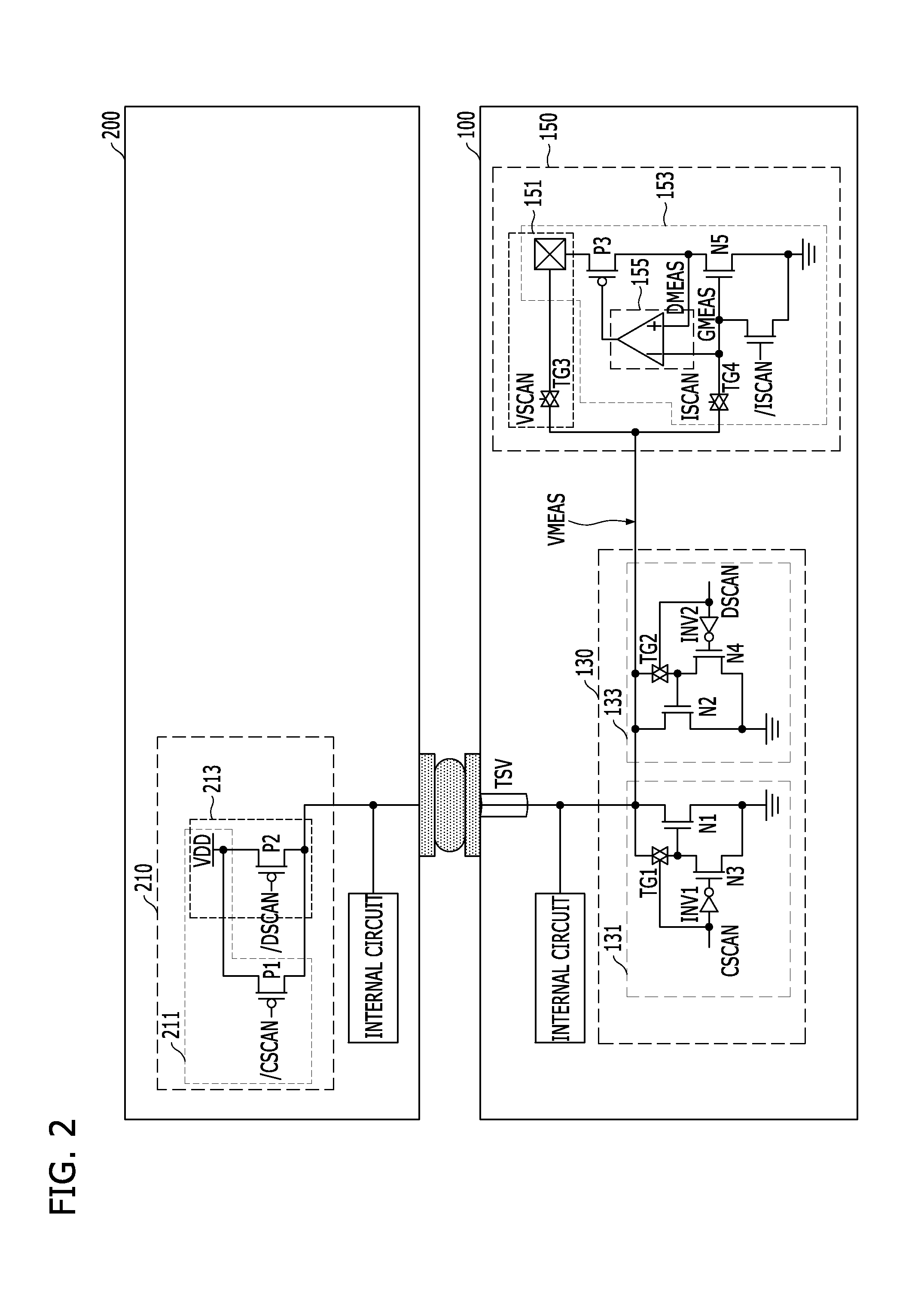
[0021]FIG. 1 is a block diagram illustrating a sem...


PUM


Abstract

A semiconductor device includes a first die, a second die coupled to the first die through a Through-Silicon-Via (TSV), and a test circuit suitable for measuring a resistance of the TSV by controlling an amount of current flowing through the TSV.

Description

CROSS-REFERENCE TO RELATED APPLICATIONS[0001]The present application claims priority of Korean Patent Application No. 10-2013-0069603, filed on Jun. 18, 2013, which is incorporated herein by reference in its entirety.BACKGROUND[0002]1. Field[0003]Exemplary embodiments of the present invention relate to a semiconductor test circuit for measuring a resistance of a Through-Silicon-Via (TSV), and a semiconductor device including the semiconductor test circuit.[0004]2. Description of the Related Art[0005]Packaging technology for a semiconductor integrated circuit has made progress continuously to satisfy the demands for minimization and reliability of the semiconductor integrated circuit. As recent products are required to realize high performance as well as small size, diverse stack packaging methods are being developed. Among them is a three-dimensional (3D) semiconductor device whose integration degree is raised by stacking a plurality of chips in a single package to achieve high inte...

Claims


Application Information

Patent Timeline
Patent Type & Authority Applications(United States)
IPC IPC(8): G01R27/14H01L21/66
CPCH01L22/34G01R27/14G01R27/205G01R31/31717G01R31/318513G11C29/025G11C29/50008H01L21/768H01L22/00
Inventor LEE, DONG-UK
Owner SK HYNIX INC
Why Eureka
Try Eureka