Phase-change memory cells

a memory cell and phase-change technology, applied in the field of phase-change memory cells, can solve the problems of destroying information, amorphous phase resistance exhibits undesirable attributes, and complicates the read out of stored information

Inactive Publication Date: 2014-12-18
GLOBALFOUNDRIES INC
View PDF1 Cites 28 Cited by
  • Summary
  • Abstract
  • Description
  • Claims
  • Application Information

AI Technical Summary

Benefits of technology

[0012]According to one aspect of the present invention, a phase-change memory cell for storing information in a plurality of programmable cell states is provided. The memory cell includes: a phase-change material located between a first electrode and a second electrode for applying a read voltage to the phase-change material to read a programmed cell state; and an electrically-conductive component extending in a direction between the first and second electrodes in contact with the phase-change material and arranged to present, to a cell current produced by the read voltage, a lower-resistance current path than an amorphous phase of the phase-change material in any of the plurality of programmable cell states, said current path having a length dependent on a size of said amorphous phase, wherein a volume of the electrically-conductive component is greater than about half that of said phase-change material.
[0013]According to a second aspect of the present invention, a memory device is provided. The memory device includes: an array of phase-change memory cells having: a phase-change material located between a first electrode and a second electrode for applying a read voltage to the phase-change material to read a programmed cell state; and an electrically-conductive component extending in a direction between the first and second electrodes in contact with the phase-change material and arranged to present, to a cell current produced by the read voltage, a lower-resistance current path than an amorphous phase of the phase-change material in any of the plurality of programmable cell states, said current path having a length dependent on a size of said amorphous phase, wherein a volume of the electrically-conductive component is greater than about half that of said phase-change material; and a read / write controller for reading and writing data in the phase-change memory cells.
[0014]According to a third aspect of the present invention, a method for forming a phase-change memory cell for storing information in a plurality of programmable cell states is provided. The method includes: forming a first electrode and a second electrodes having a phase-change material located there between; and forming an electrically-conductive component having a volume which is greater than half that of said phase-change material, wherein said electrically-conductive component extends in a direction between the first and second electrodes in contact with the phase-change material and is arranged to present, to a cell current produced by a read voltage applied via the first and second electrodes to read a programmed cell state in use, a lower-resistance current path than an amorphous phase of the phase-change material in any of said plurality of programmable cell states, said current path having a length dependent on a size of said amorphous phase.

Problems solved by technology

A problem with phase-change memory is that the resistance of the amorphous phase exhibits undesirable attributes such as low-frequency noise and drift.
This complicates read out of the stored information, potentially even destroying the information if there is a large variability in the drift exhibited by different cell states so that the read measurement distributions for neighboring cell states interfere with one another.
The larger the number of cell states, and so closer the initial spacing between readback resistance levels, the more susceptible cells are to this problem.
This presents a significant challenge in the development of multilevel phase-change memory, frustrating efforts to achieve storage of more bits per cell for increased storage density and so reduce manufacturing cost per bit.
These methods typically incur a penalty in write or read speed, and require more complicated read / write circuitry for the memory cells.
This inherently reduces storage density.
Various other problems are associated with current PCM cells.
This has an adverse effect on power consumption.
Thermal disturb is another key problem faced by phase-change memory as cell-size is reduced.
This presents a significant technological challenge to the future scaling of PCM.

Method used


Image

  • Phase-change memory cells
  • Phase-change memory cells
  • Phase-change memory cells

Examples


Embodiment Construction

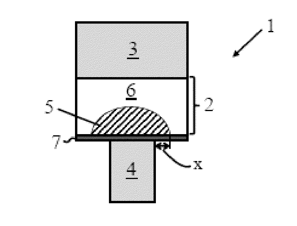
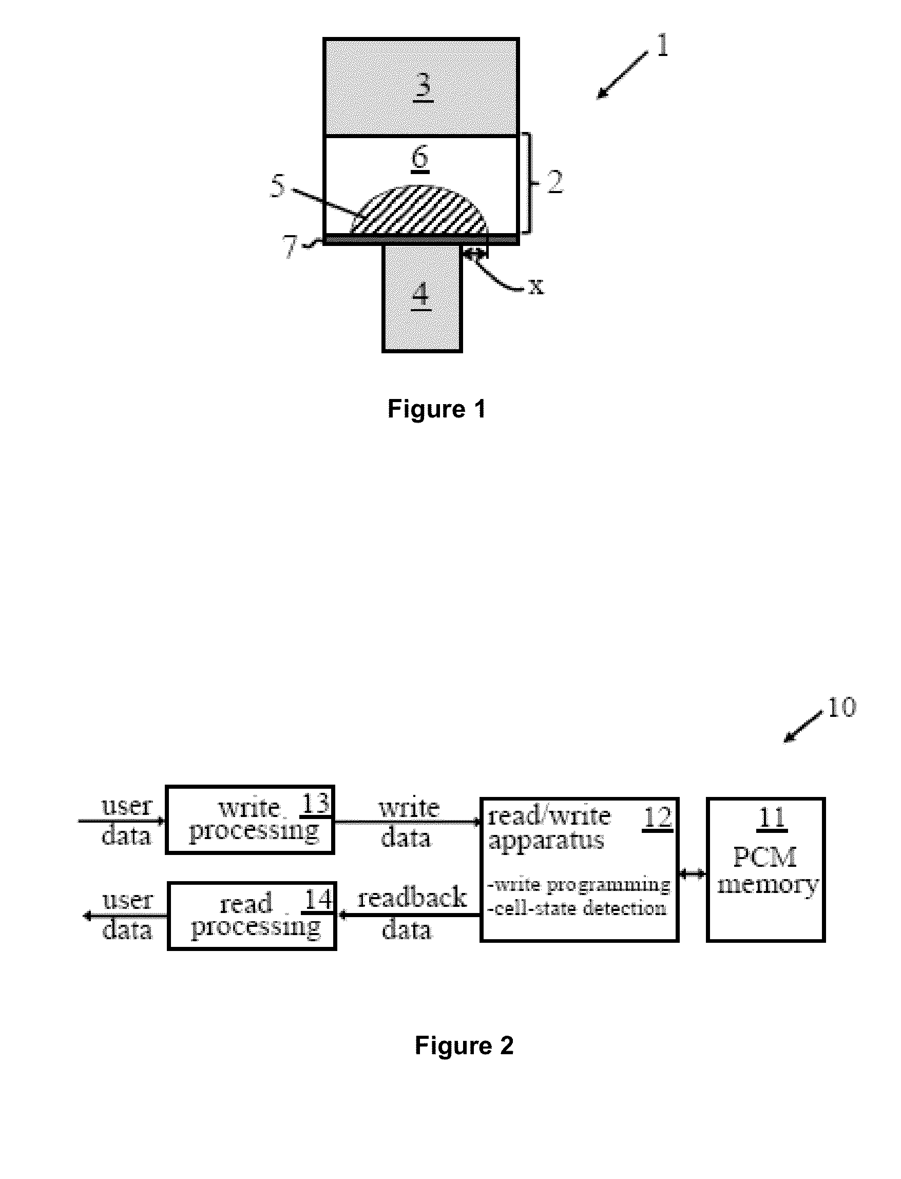
[0035]FIG. 2 is a simplified schematic of a phase-change memory device, according to an embodiment of the present invention. Device 10 includes multilevel phase-change memory 11 for storing data in one or more integrated arrays of PCM cells described below. Reading and writing of data to memory 11 is performed by a read / write controller 12. Controller 12 includes circuitry of generally known form for programming PCM cells during data write operations and making read measurements for detecting cell-state during data read operations. During these operations, the read / write controller can address individual PCM cells by applying appropriate control signals to an array of word and bit lines in memory ensemble 11. As indicated by block 13 in the figure, user data input to device 10 is typically subjected to some form of write-processing, such as coding for error-correction purposes, before being supplied as write data to controller 12. Similarly, readback data output by controller 12 is ...


PUM


Abstract

A phase-change memory cell for storing information in a plurality of programmable cell states. The memory cell includes: a phase-change material located between a first electrode and a second electrode for applying a read voltage to the phase-change material to read a programmed cell state; and an electrically-conductive component extending in a direction between the first and second electrodes in contact with the phase-change material and arranged to present, to a cell current produced by the read voltage, a lower-resistance current path than an amorphous phase of the phase-change material in any of the plurality of programmable cell states, said current path having a length dependent on a size of said amorphous phase, wherein a volume of the electrically-conductive component is greater than about half that of said phase-change material.

Description

CROSS-REFERENCE TO RELATED APPLICATION[0001]This application claims priority under 35 U.S.C. §119 from GB Patent Application No. 1310629.9 filed Jun. 14, 2013, the entire contents of which are incorporated herein by reference.BACKGROUND OF THE INVENTION[0002]1. Field of the Invention[0003]The present invention relates to phase-change memory cells.[0004]2. Description of Related Art[0005]Phase-change memory (PCM) is a non-volatile solid-state memory technology that exploits the reversible, thermally-assisted switching of phase-change materials, in particular chalcogenide compounds such as GST (Germanium-Antimony-Tellurium), between states with different electrical resistance. The fundamental storage unit (the “cell”) can be programmed into a number of different states, or levels, which exhibit different resistance characteristics. The s programmable cell-states can be used to represent different data values, permitting storage of information.[0006]In single-level PCM devices, each ce...

Claims


Application Information

Patent Timeline
Patent Type & Authority Applications(United States)
IPC IPC(8): G11C13/00H01L45/00
CPCG11C13/0004H01L45/16H01L45/12H01L45/06G11C13/003G11C13/004G11C2213/50H10N70/823H10N70/231H10N70/861H10N70/826H10N70/8828H10N70/066G11C11/5678H10N70/011H10N70/801
Inventor KREBS, DANIELSEBASTIAN, ABU
Owner GLOBALFOUNDRIES INC
Why Eureka
Try Eureka