Arrayed waveguide grating, optical module provided with said arrayed waveguide grating, and optical communications system
a technology of arrayed waveguides and optical modules, applied in the field of arrayed waveguides, can solve the problems of increasing system upgrade costs, difficulty in realizing them, and inability to realize narrow wavelength intervals in the 1.5 m band, and achieve the effect of low cost and low cos
- Summary
- Abstract
- Description
- Claims
- Application Information
AI Technical Summary
Benefits of technology
Problems solved by technology
Method used
Image
Examples
first embodiment
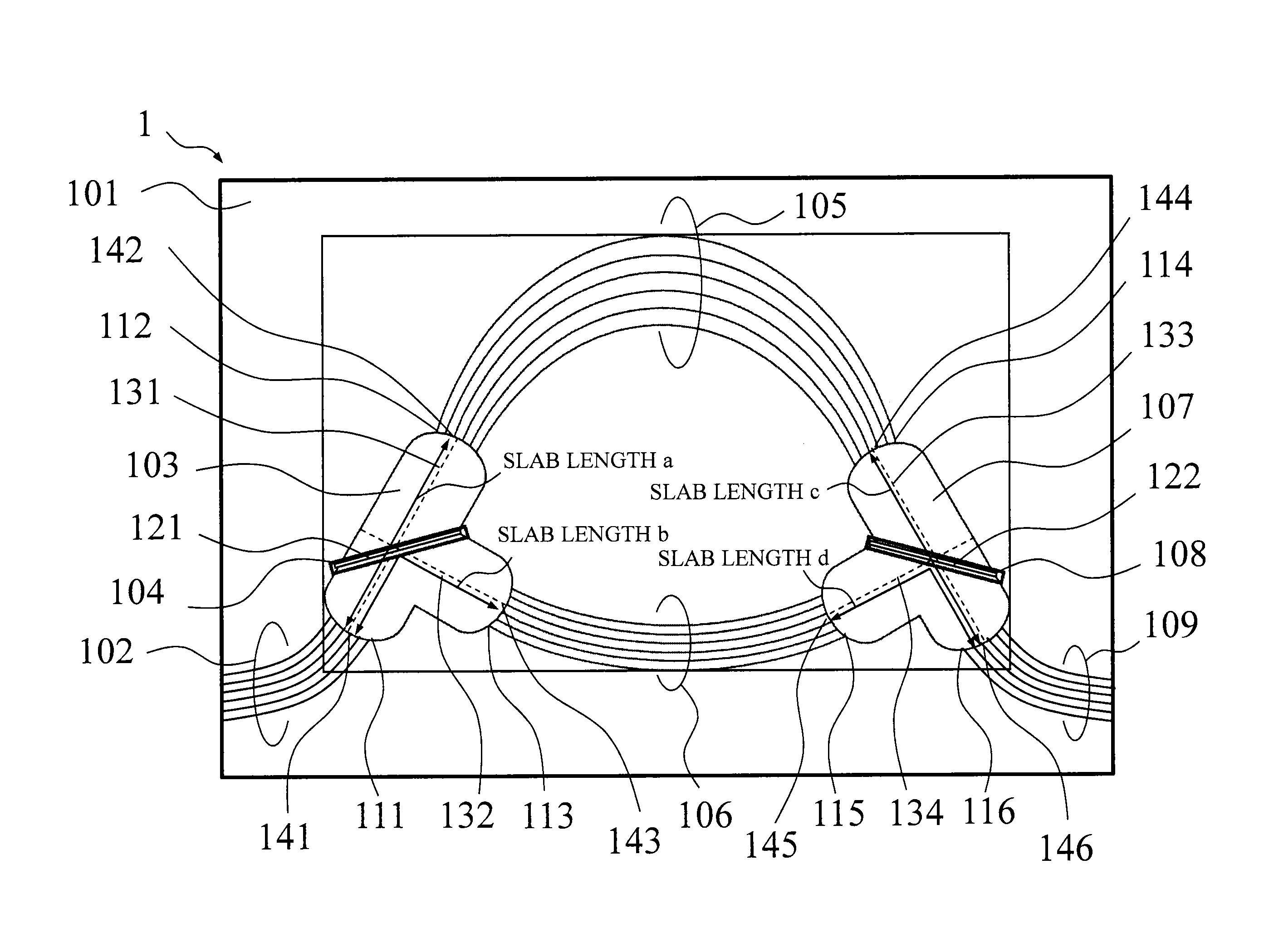
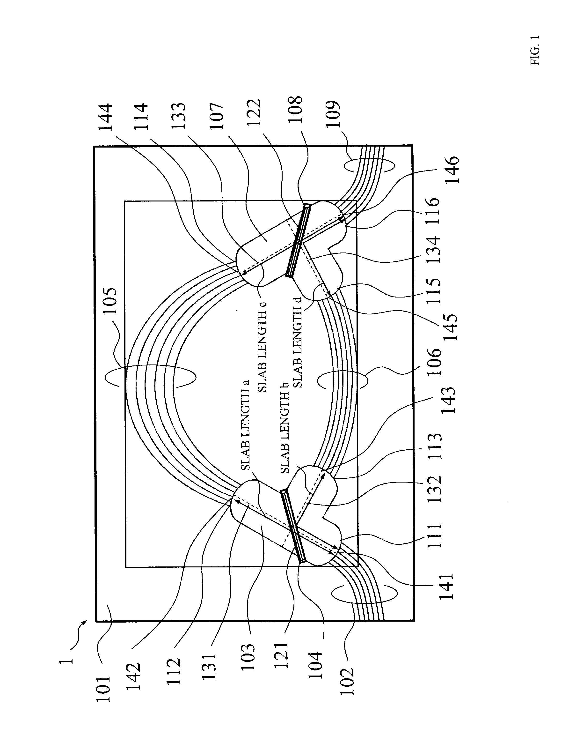
[0068]FIG. 1 is a schematic diagram of an aspect of an arrayed waveguide grating 1 according to the first embodiment of the present invention. As illustrated in FIG. 1, the arrayed waveguide grating 1 according to a first embodiment of the present invention is a both-side input / output waveguide integrated arrayed waveguide grating 1 in which a first slab waveguide 103, a second slab waveguide 107, a first input / output waveguide 102 connected to the first slab waveguide 103, a second input / output waveguide 109 connected to the second slab waveguide 107, a first channel waveguide group 105 with both ends connected to the first slab waveguide 103 and the second slab waveguide 107, and a second channel waveguide group 106 with both ends connected to the first slab waveguide 103 and the second slab waveguide 107 are formed on a substrate 101 formed of a silicon substrate, a glass substrate and the like.
[0069]Each of the first channel waveguide group 105 and the second channel waveguide g...
second embodiment
[0114]A second embodiment of the present invention is hereinafter described in detail with reference to the attached drawings. Meanwhile, in the following description, the same reference sign is assigned to the similar structure and the same member as those of the above-described first embodiment and detailed description thereof is omitted or the description is simplified.
[0115]FIG. 12 is a schematic diagram of an aspect of an arrayed waveguide grating 2 according to the second embodiment of the present invention. As illustrated in FIG. 12, the arrayed waveguide grating 2 according to the second embodiment of the present invention is a single-side input / output waveguide integrated arrayed waveguide grating 2 in which a first slab waveguide 203, a second slab waveguide 207, a first input / output waveguide 202 connected to the first slab waveguide 203, two second input / output waveguides 209 and 210 connected to the second slab waveguide 207, a first channel waveguide group 205 with bot...
third embodiment
[0141]An example of an optical communications system Z1 in which an arrayed waveguide grating 1 according to the present invention is used is hereinafter described with reference to the drawings.
[0142]FIG. 15 is a schematic diagram of an aspect of the optical communications system Z1 in which the arrayed waveguide grating 1 according to a first embodiment of the present invention is used. The optical communications system Z1 illustrated in FIG. 15 is a wavelength-variable WDM / TDM-PON in which a wavelength band and a wavelength interval of upstream are different from those of downstream in which a both-side input / output waveguide integrated arrayed waveguide grating 1 according to the first embodiment is used.
[0143]The optical communications system Z1 illustrated in FIG. 15 is formed of the arrayed waveguide grating 1, a subscriber device 401, a station side device 501, and optical fibers F1 to F3 connecting them in which a plurality of subscriber devices 401 is connected to each por...
PUM
 Abstract
Description
Claims
Application Information


