
Monolithic ceramic electronic component

a technology of electronic components and monolithic ceramics, applied in the direction of fixed capacitor details, generators/motors, fixed capacitors, etc., can solve the problems of easy short circuit failure, short circuit failure, short circuit failure, etc., and achieve the effect of significantly reducing or preventing short circuit failures, and increasing thickness

Active Publication Date: 2015-01-01
MURATA MFG CO LTD
View PDF13 Cites 14 Cited by
  • Summary
  • Abstract
  • Description
  • Claims
  • Application Information

AI Technical Summary

Benefits of technology

The present invention provides a monolithic ceramic electronic component that prevents short circuit failures caused by unintended movement of conductive adhesive or formation of connections between outer electrodes through conductive adhesive. This is achieved by using Pd electrodes or Pd-Ni alloy electrodes as the outermost layers of the outer electrodes, which do not contain Ag. The thickness of the intermediate electrode layer on the main surfaces and side surfaces of the ceramic body is larger than the thickness of the intermediate electrode layer on the end surfaces of the ceramic body, ensuring a sufficient distance between the lowermost point of the outer electrodes in the mounting surface of the monolithic ceramic electronic component and the surface of the ceramic body. This mounting structure prevents short circuit failures and also prevents electrochemical migration of Ag.

Problems solved by technology

However, in the monolithic ceramic electronic component described in Japanese Unexamined Patent Application Publication No. 2002-158137, electrochemical migration of Ag may cause short circuit failures between outer electrodes.
In such an atmosphere, short circuit failures easily occur in the monolithic ceramic electronic component described in Japanese Unexamined Patent Application Publication No. 2002-158137 due to electrochemical migration of Ag.
As a result, the conductive adhesive 3 may form a connection between outer electrodes 6, causing short circuit failures.

Method used


Image

  • Monolithic ceramic electronic component
  • Monolithic ceramic electronic component
  • Monolithic ceramic electronic component

Examples


examples

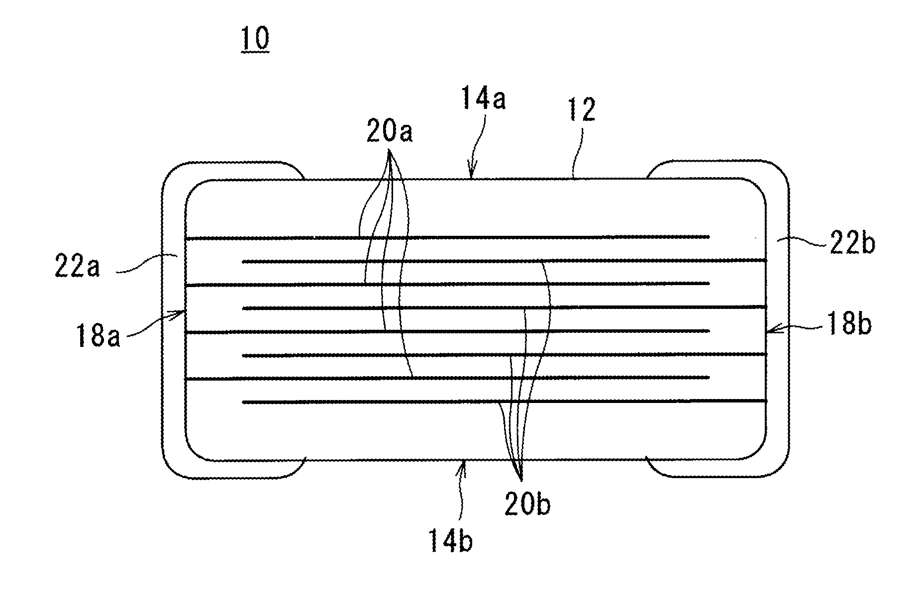
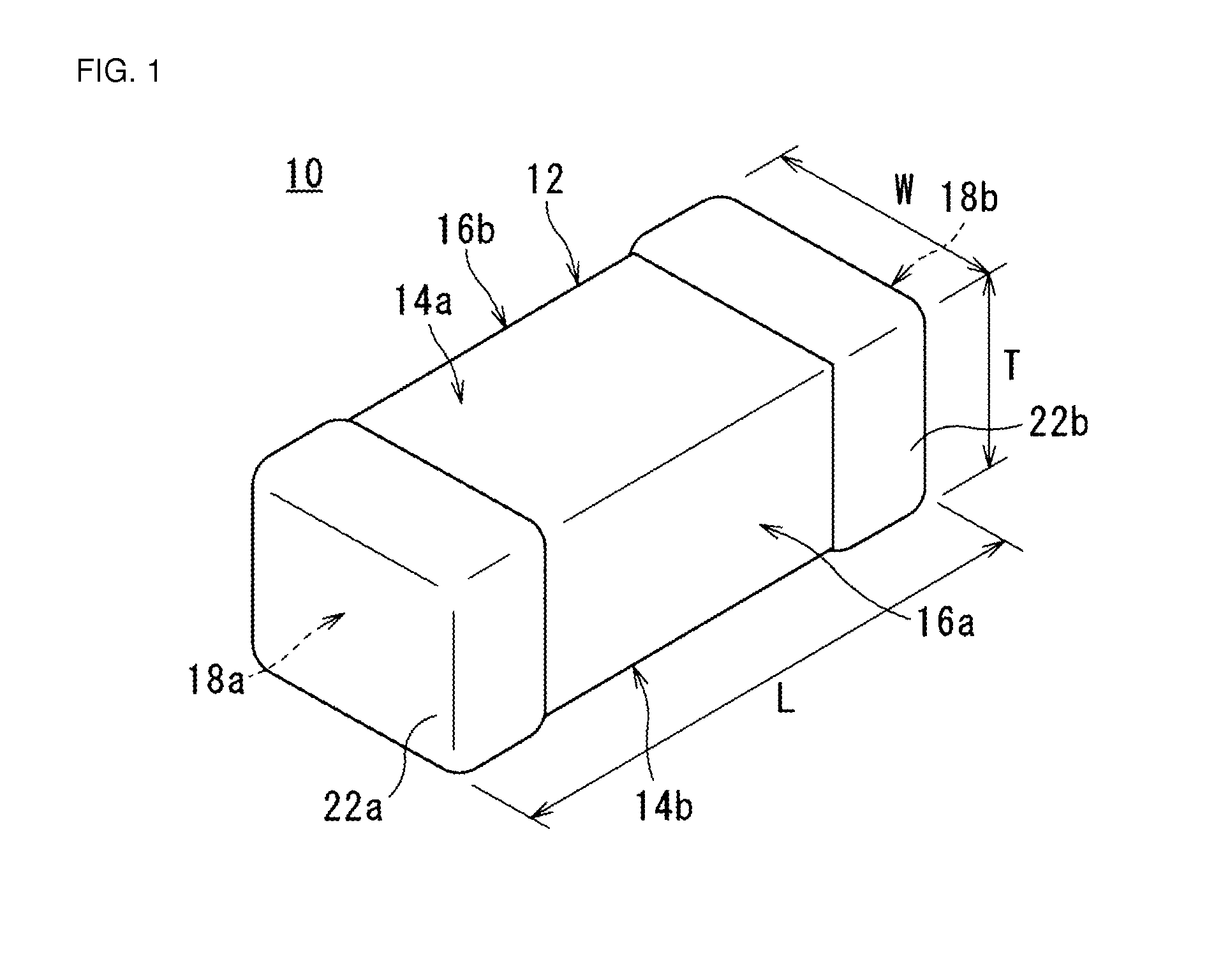
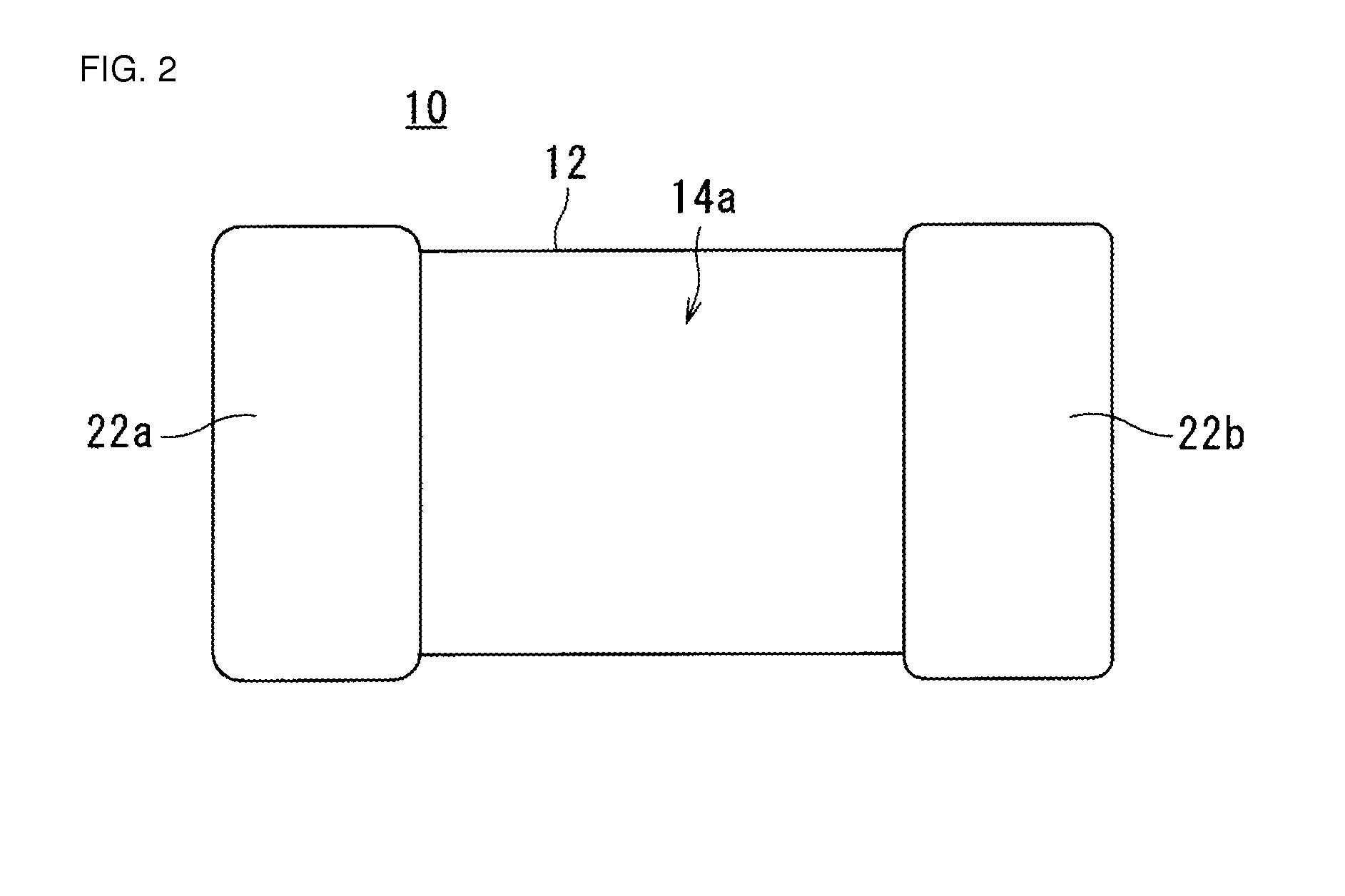
[0051]An example of a ceramic body for a monolithic ceramic capacitor was prepared. This ceramic body included ceramic layers formed of BaTiO3 and inner electrodes formed of Ni and had chip dimensions (L×W×T) of approximately 1.0 mm×0.5 mm×0.5 mm. Lower electrode layers were formed of Cu and had a thickness of about 30 μm on the central portions of the end surfaces of the ceramic body and had a thickness of about 5 μm on the main surfaces and the side surfaces of the ceramic body. Intermediate electrode layers had a thickness of about 5 μm on the central portions of the end surfaces of the ceramic body. Upper electrode layers had a thickness of about 0.1 μm on the central portions of the end surfaces of the ceramic body and had a thickness of about 0.1 μm on the main surfaces and the side surfaces of the ceramic body. The intermediate electrode layers were formed as Ni plating layers by Ni plating in Watts bath with about 0.5-mm-diameter media for approximately 60 minutes. The other...


PUM

PropertyMeasurementUnit
distanceaaaaaaaaaa
temperatureaaaaaaaaaa
distanceaaaaaaaaaa

Abstract

A monolithic ceramic electronic component includes a ceramic body including a stack of ceramic layers. Inner electrodes are disposed within the ceramic body and include exposed portions at the end surfaces of the ceramic body. A pair of outer electrodes is arranged on the end surfaces of the ceramic body so as to extend from the end surfaces to the main surfaces and side surfaces of the ceramic body. Each of the outer electrodes includes a lower electrode layer provided on the ceramic body, an intermediate electrode layer located on the lower electrode layer and defined by a plated Ni layer, and an upper electrode layer located on the intermediate electrode layer and defined by a plated Pd layer. A thickness of the intermediate electrode layer on the main surfaces and the side surfaces of the ceramic body is larger than a thickness of the intermediate electrode layer on the end surfaces of the ceramic body.

Description

BACKGROUND OF THE INVENTION[0001]1. Field of the Invention[0002]The present invention relates to a monolithic ceramic electronic component, and particularly to, for example, a monolithic ceramic electronic component in which outer electrodes are provided on both end surfaces of a multilayer body.[0003]2. Description of the Related Art[0004]In recent years, a large number of electronic components such as ceramic electronic components have come to be mounted on circuit substrates installed in electronic equipment. For mounting such electronic components on circuit substrates, Pb-containing solder has been commonly used. However, in recent years, in order to reduce environmental loads, studies on Pb-free mounting of electronic components have been increasingly performed.[0005]In a known example of a Pb-free method of mounting electronic components on circuit substrates, electronic components are mounted with Pb-free solder or a conductive adhesive containing a thermosetting resin such ...

Claims


Application Information

Patent Timeline
Patent Type & Authority Applications(United States)
IPC IPC(8): H01F27/28H01G2/06H01C7/00H01G4/012H01G4/30H01L41/047H10N30/50H10N30/87H10N30/88
CPCH01C7/008H01G4/30H01G4/012H01F2027/2809H01F27/2804H01L41/0471H01G2/065H01F27/292H01G4/12H01G4/232H01L41/0475H01L41/053H10N30/871H10N30/875H10N30/88H10N30/50H10N30/877H01F27/245
Inventor KATSUTA, SEIJIKAINUMA, YASUAKINAGAOKA, TATSUYAMOTOKI, AKIHIROKODAMA, SATOSHI
Owner MURATA MFG CO LTD
Learn More