Matrix defined electrical circuit structure

a technology of electrical circuit and matrix, applied in the field of matrix defined electrical circuit structure, can solve the problems of rigid pcb products, rigid pcb products, and limited layer count or feature registration, and achieve the effects of reducing parasitic electrical effects and impedance mismatch, dense functionalized structures, and increasing current carrying capacity

Inactive Publication Date: 2015-01-15
HSIO TECH
View PDF40 Cites 41 Cited by
  • Summary
  • Abstract
  • Description
  • Claims
  • Application Information

AI Technical Summary

Benefits of technology

[0014]The printed circuit can be produced to replicate a traditional circuit or interconnects between one or more members of a system. The present system permits circuit structures to be produced digitally, without tooling or costly artwork. The circuit structures can be produced as a “Green” product, with dramatic reductions in environmental issues related to the production of conventional flexible circuits.
[0025]The compliant printed flexible circuit can be configured with conductive traces that reduce or redistribute the terminal pitch, without the addition of an interposer or daughter substrate. Grounding schemes, shielding, electrical devices, and power planes can be added to the interconnect assembly, reducing the number of connections to the PCB and relieving routing constraints while increasing performance.

Problems solved by technology

They can be considered expensive compared to some rigid PCB products.
They do have some limitations regarding layer count or feature registration, and they are generally used for small or elongated applications.
Rigid PCB's and package substrates experience challenges as the feature sizes and line spacing are reduced to achieve further miniaturization and increased circuit density.
As density increases, the laser processed via structures can experience significant taper, carbon contamination, layer to layer shorting during the plating process due to registration issues, and high resistance interconnections that may be prone to result in reliability issues.
The challenge of making fine line PCBs often relates to the difficulty in creating very small or blind and buried vias.

Method used


Image

  • Matrix defined electrical circuit structure
  • Matrix defined electrical circuit structure
  • Matrix defined electrical circuit structure

Examples


Embodiment Construction

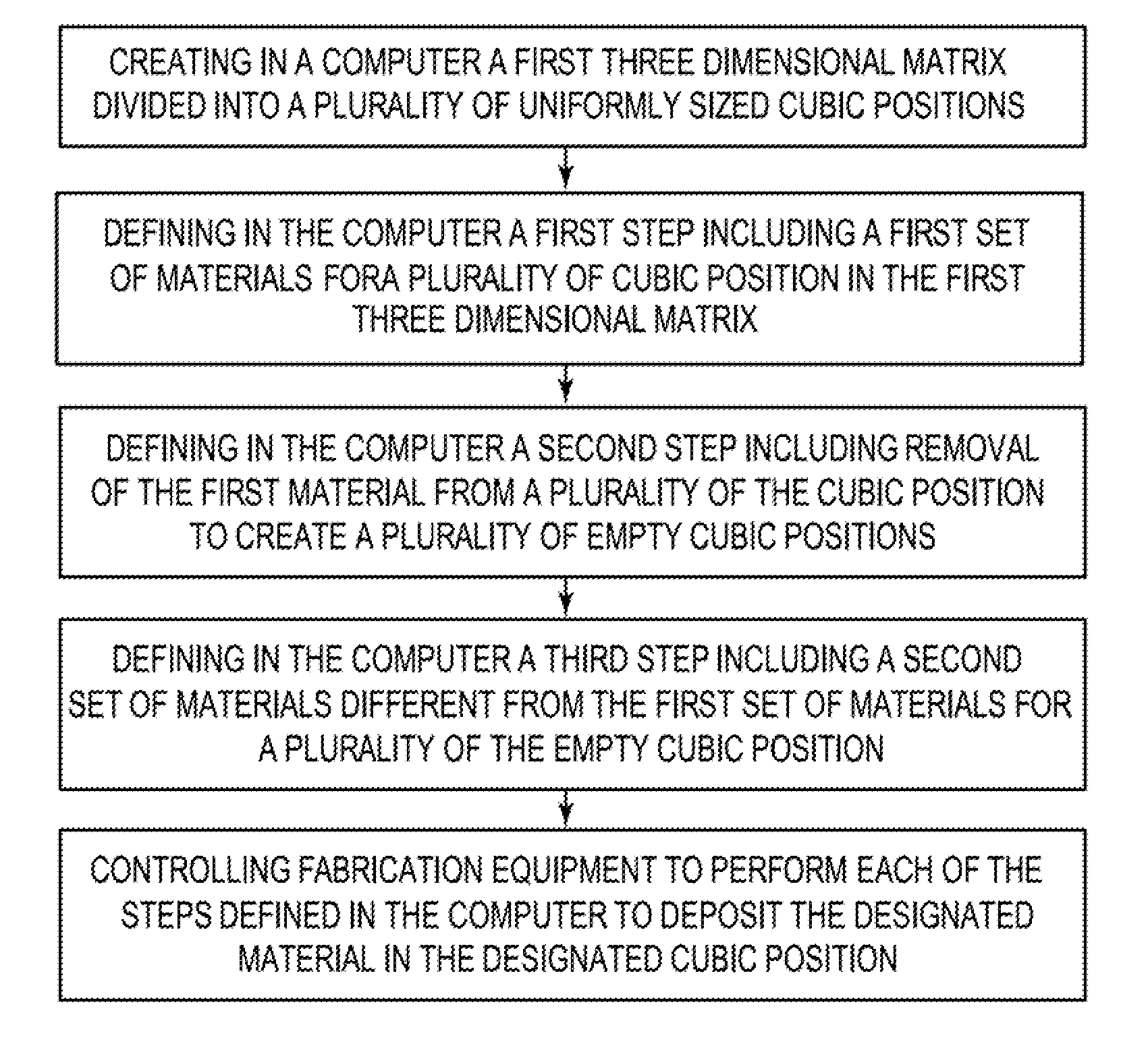
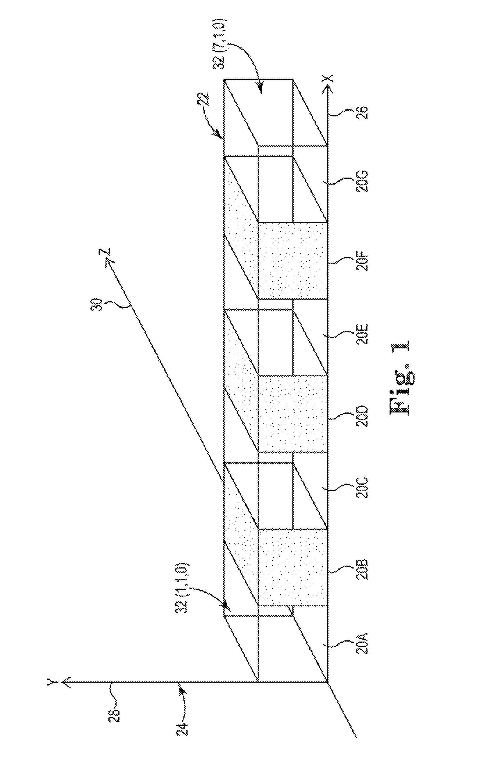
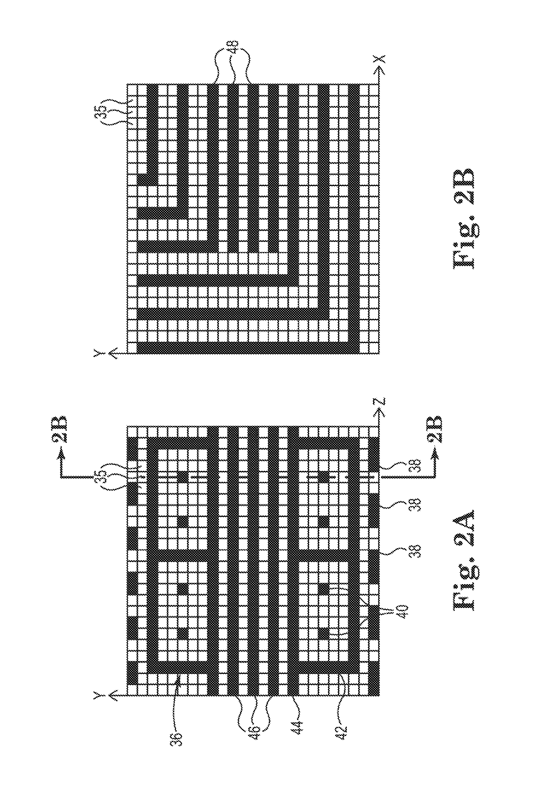
[0050]The present disclosure is directed to a system for “pixelating” a three-dimensional circuit structure into a three-dimensional matrix of cubes that are located with respect to a coordinate system. The present system and method can be used to both design and fabricate the circuit structures. The fabrication process involves adding and removing bulk materials from the individual cubic units within the pixelated representation of the circuit structure.

[0051]Various existing and new techniques are used to add or subtract bulk materials as the cubic positions within the matrix to construct the circuit structure, including U.S. Ser. No. 13 / 413,724, entitled Copper Pillar Full Metal Via Electrical Circuit Structure filed Mar. 7, 2012; U.S. Ser. No. 13 / 410,943 entitled Area Array Semiconductor Device Package Interconnect Structure with Optional Package-to-Package or Flexible Circuit to Package Connection, filed Mar. 2, 2012; U.S. Ser. No. 13 / 700,639 entitled Electrical Connector Insul...


PUM

PropertyMeasurementUnit
sizeaaaaaaaaaa
dielectric constantaaaaaaaaaa
aspect ratioaaaaaaaaaa

Abstract

A system and method for “pixelating” a three-dimensional circuit structure into a three-dimensional matrix of cubes that are located with respect to a coordinate system. The design step is typically performed on a conventional computer using computer aided design software that pixelates the proposed circuit structure into an array of uniformly sized cube. The fabrication process involves adding and subtracting bulk materials from the individual cubic positions within the pixelated representation of the circuit structure. Various existing and new techniques can be used to add or subtract bulk materials as the cubic positions within the matrix to construct the circuit structure.

Description

CROSS-REFERENCE TO RELATED APPLICATIONS[0001]This application claims the benefit of U.S. Provisional Application No. 61 / 845,076, filed Jul. 11, 2013, the disclosure of which is hereby incorporated by reference.TECHNICAL FIELD[0002]The present disclosure relates to a system and method for designing and fabricating circuit structures by adding and subtracting bulk materials from individual cubic units within a pixelated representation of the circuit structure. The present disclosure leverages processes used in the printed circuit and semiconductor packaging industries to provide a high performance electrical interconnect between two or more components in an electrical system.BACKGROUND OF THE INVENTION[0003]Traditional printed circuits are often constructed in what is commonly called rigid or flexible formats. The rigid versions are used in nearly every electronic system, where the printed circuit board (PCB) is essentially a laminate of materials and circuits that when built is relat...

Claims


Application Information

Patent Timeline
Patent Type & Authority Applications(United States)
IPC IPC(8): H05K3/46H05K3/12H01L21/768H05K3/18
CPCH05K3/12H05K3/181H05K3/188H01L21/76877H05K3/4611H05K1/0393H05K1/16H05K3/0005H05K3/4069H05K3/421H05K3/429H05K3/465H05K3/4658H05K2201/09272H05K2201/09509H05K2201/09536H05K2201/098H05K2203/013H05K2203/1476H01L2224/16225H01L2224/48091H01L2224/48227H01L2924/15311B33Y80/00H01L2924/00014
Inventor RATHBURN, JAMES
Owner HSIO TECH
Why Eureka
Try Eureka