Film formation device and film formation method for forming metal film

a metal film and film formation technology, applied in contact devices, electrolysis components, electrolysis processes, etc., can solve the problem of limit in increasing the thickness of the film

Active Publication Date: 2015-01-15
TOYOTA JIDOSHA KK
View PDF8 Cites 37 Cited by
  • Summary
  • Abstract
  • Description
  • Claims
  • Application Information

AI Technical Summary

Benefits of technology

[0038]According to the present invention, metal films with a desired thickness can be continuously formed on the surfaces of a plurality of substrates.

Problems solved by technology

Thus, there is a limitation in increasing the thickness of the film.

Method used


Image

  • Film formation device and film formation method for forming metal film
  • Film formation device and film formation method for forming metal film
  • Film formation device and film formation method for forming metal film

Examples


first embodiment

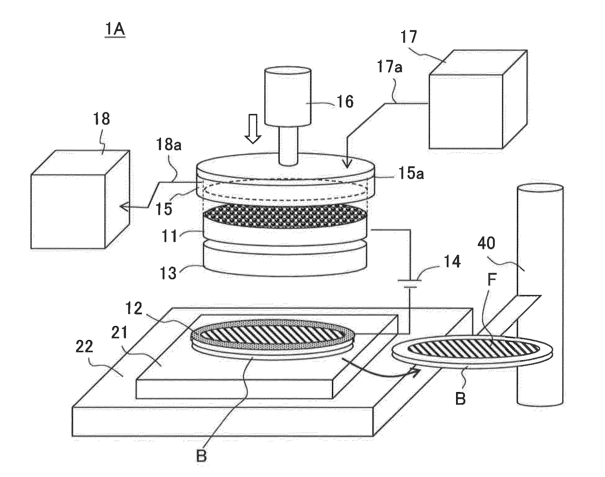
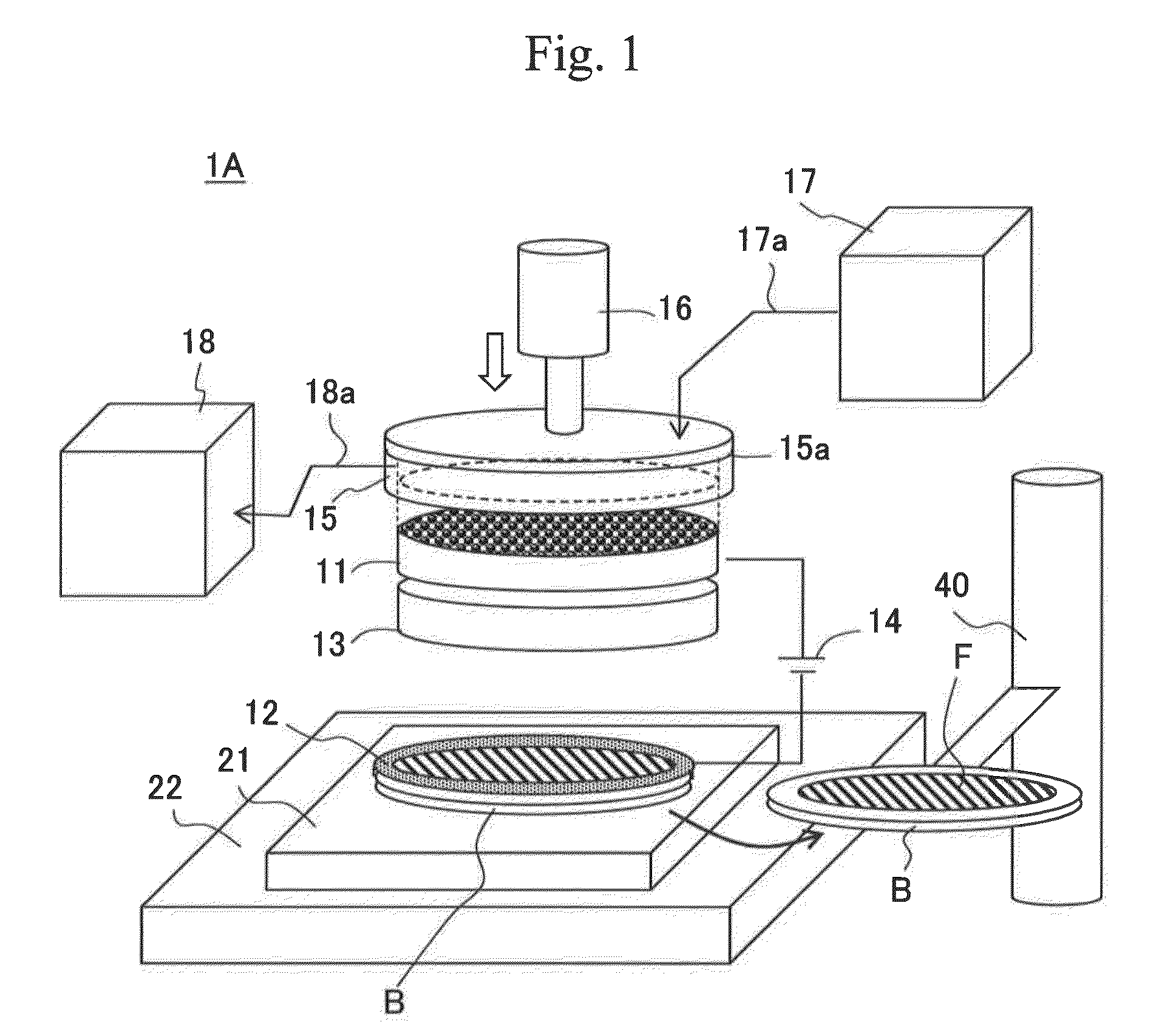
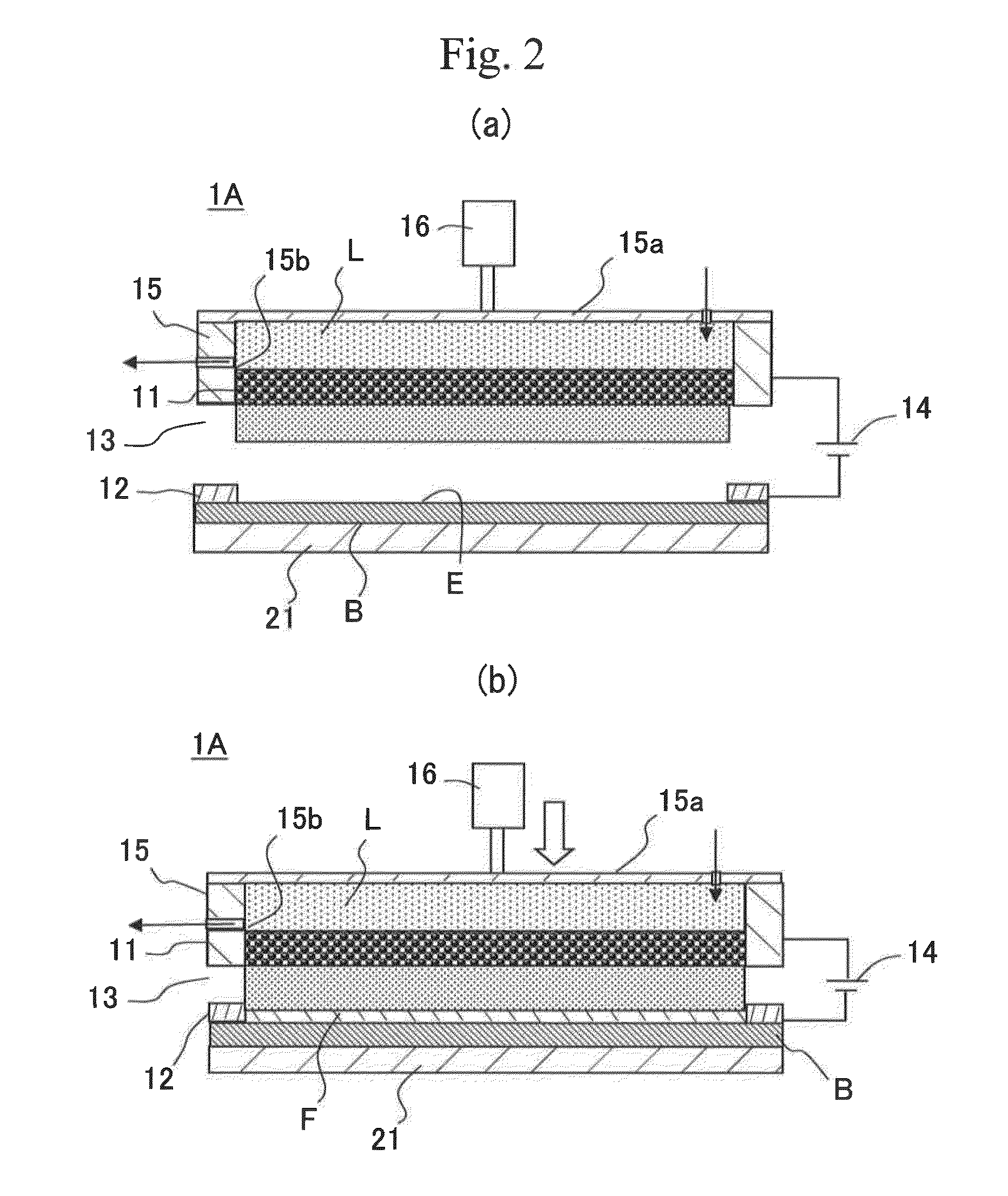
[0049]FIG. 1 is a schematic conceptual view of a film formation device for forming a metal film in accordance with a first embodiment of the present invention. FIGS. 2 are views illustrating a film formation method that uses the film formation device for forming a metal film shown in FIG. 1; specifically, FIG. 2(a) is a schematic cross-sectional view illustrating the state of the film formation device before formation of a film, and FIG. 2(b) is a schematic cross-sectional view illustrating the state of the film formation device during formation of a film.

[0050]As illustrated in FIG. 1, a film formation device IA in accordance with the present invention is a device that deposits metal from metal ions and thus forms a metal film made of the deposited metal on the surface of a substrate B. Herein, for the substrate B, a substrate made of a metal material such as aluminum, or a substrate obtained by forming a metal baser layer on a surface, which is to be processed, of a resin or silic...

second embodiment

[0070]FIG. 3 is a schematic cross-sectional view of a film formation device for forming a metal film in accordance with a second embodiment of the present invention. FIG. 4 is a schematic plan view of a bottom face of the film formation device shown in FIG. 3. FIG. 5 is a cross-sectional view illustrating the structure of a conducting portion (i.e., conducting protrusions) of the film formation device shown in FIG. 3. FIG. 6 is a schematic cross-sectional view illustrating the state of the film formation device shown in FIG. 3 during formation of a film.

[0071]The second embodiment differs from the first embodiment in the structure of the conducting portion of the film formation device and in that an insulating member is newly provided. Accordingly, structures that are common to those in the first embodiment are denoted by the same reference numerals, and detailed description thereof will be omitted.

[0072]As illustrated in FIG. 3, a film formation device 1B in accordance with the sec...

fourth embodiment

[0097]FIG. 8 is a schematic cross-sectional view illustrating a pretreatment step of a film formation device for forming a metal film in accordance with a fourth embodiment of the present invention, The fourth embodiment differs from the first embodiment in that an acid aqueous solution (i.e., an electrolytic solution) is stored as a solution stored in the metal ion supply unit instead of the metal ion solution. L. Accordingly, structures that are common to those in the first embodiment are denoted by the same reference numerals, and detailed description thereof will be omitted.

[0098]As a substrate B shown in FIG. 8, a substrate made of aluminum, an aluminum alloy, or the like, or a substrate having an oxide film BR formed thereon is used, for example. It should be noted that when a substrate made of aluminum, an aluminum alloy, or the like is used, an oxide film BR is formed as a passivation film on the surface of the substrate.

[0099]As described above, when an oxide film BR is for...


PUM

PropertyMeasurementUnit
thicknessaaaaaaaaaa
pore sizeaaaaaaaaaa
oxygen overvoltageaaaaaaaaaa

Abstract

Provided are a film formation device and a film formation method for forming a metal film, with which metal films with a desired thickness can be continuously formed on surfaces of a plurality of substrates. A film formation device 1A includes at least a positive electrode 11, a negative electrode 12, a solid electrolyte membrane 13 arranged on a surface of the positive electrode 12, between. the positive electrode and a substrate to serve as the negative electrode, and a power supply unit E adapted to apply a voltage across the positive electrode 11 and the substrate B. A voltage is applied across the positive electrode 11 and the substrate B to deposit metal on a surface of the substrate from metal ions contained in the solid electrolyte membrane 13, whereby a metal film F made of metal is formed, The positive electrode 11 is made of a porous body that allows a solution L containing metal ions to pass therethrough and supplies the metal ions to the solid electrolyte membrane 13.

Description

TECHNICAL FIELD[0001]The present invention relates to a film formation device and a film formation method for forming a metal film. In particular, the present invention relates to a film formation device and a film formation method for forming a metal film, with which a thin metal film can be uniformly formed on the surface of a substrate.BACKGROUND ART[0002]Conventionally, when an electronic circuit board or the like is produced, it has been common to form a metal film on the surface of a substrate to form a metallic circuit pattern thereon. For example, as a film formation technology for forming such a metal film, there has been proposed a film formation technology that includes forming a metal film on the surface of a Si semiconductor substrate or the like through a plating process such as an electroless plating process (for example, see Patent Literature 1), or forming a metal film using PVD such as sputtering.[0003]However, when a plating process such as an electroless plating ...

Claims


Application Information

Patent Timeline
Patent Type & Authority Applications(United States)
IPC IPC(8): C25D17/00C25D21/14
CPCC25D21/14C25D17/00C25D3/00C25D3/38C25D5/02C25D5/022C25D5/08C25D5/34C25D17/005C25D17/12C25D17/14
Inventor HIRAOKA, MOTOKIYANAGIMOTO, HIROSHISATO, YUKIYOSHIOKA, TAKAYASU
Owner TOYOTA JIDOSHA KK
Why Eureka
Try Eureka