Eureka AIR delivers breakthrough ideas for toughest innovation challenges, trusted by R&D personnel around the world.

Dual conversion gain image sensor cell

Active Publication Date: 2015-01-22
STMICROELECTRONICS INT NV
View PDF4 Cites 3 Cited by
  • Summary
  • Abstract
  • Description
  • Claims
  • Application Information

AI Technical Summary

Benefits of technology

This patent provides an image sensor cell with two conductivity types, where the read region is a second conductivity type and can be used to receive a first voltage to invert its conductivity type. An adjacent storage region is also of the second conductivity type and can be used as an extension of the read region or can be set to not inversion. The sensor cell can also have a photodiode and a reset transistor, as well as a read stage for reading data from the sensor. The patent also describes an image sensor comprising multiple cells of this type. The technical effects of this patent are improved image sensor performance and flexibility in voltage application for inversion or no inversion of the sensor region.

Problems solved by technology

Thus, a read node of low capacitance enables to relatively easily discriminate low illumination variations, especially in low illumination conditions, but may however be unable to receive all the charges photogenerated in the photodiode in case of a strong illumination.
Conversely, a read node of high capacitance enables to measure high illumination levels, but does not enable to easily discriminate low illumination level variations, especially in low illumination conditions.

Method used


Image

  • Dual conversion gain image sensor cell
  • Dual conversion gain image sensor cell
  • Dual conversion gain image sensor cell

Examples


Embodiment Construction

[0023]For clarity, the same elements have been designated with the same reference numerals in the different drawings and, further, as usual in the representation of integrated circuits, the various drawings are not to scale. Further, in the following description, unless otherwise indicated, terms “approximately”, “substantially”, “around”, and “on the order of” mean “to within 10%”, and terms referring to directions, such as overhanging, covering, topping, lateral, above, under, etc., apply to circuits arranged as illustrated in the cross-section views of the corresponding drawings.

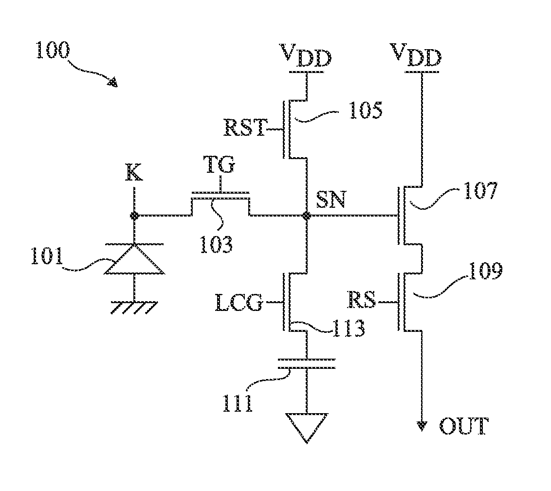
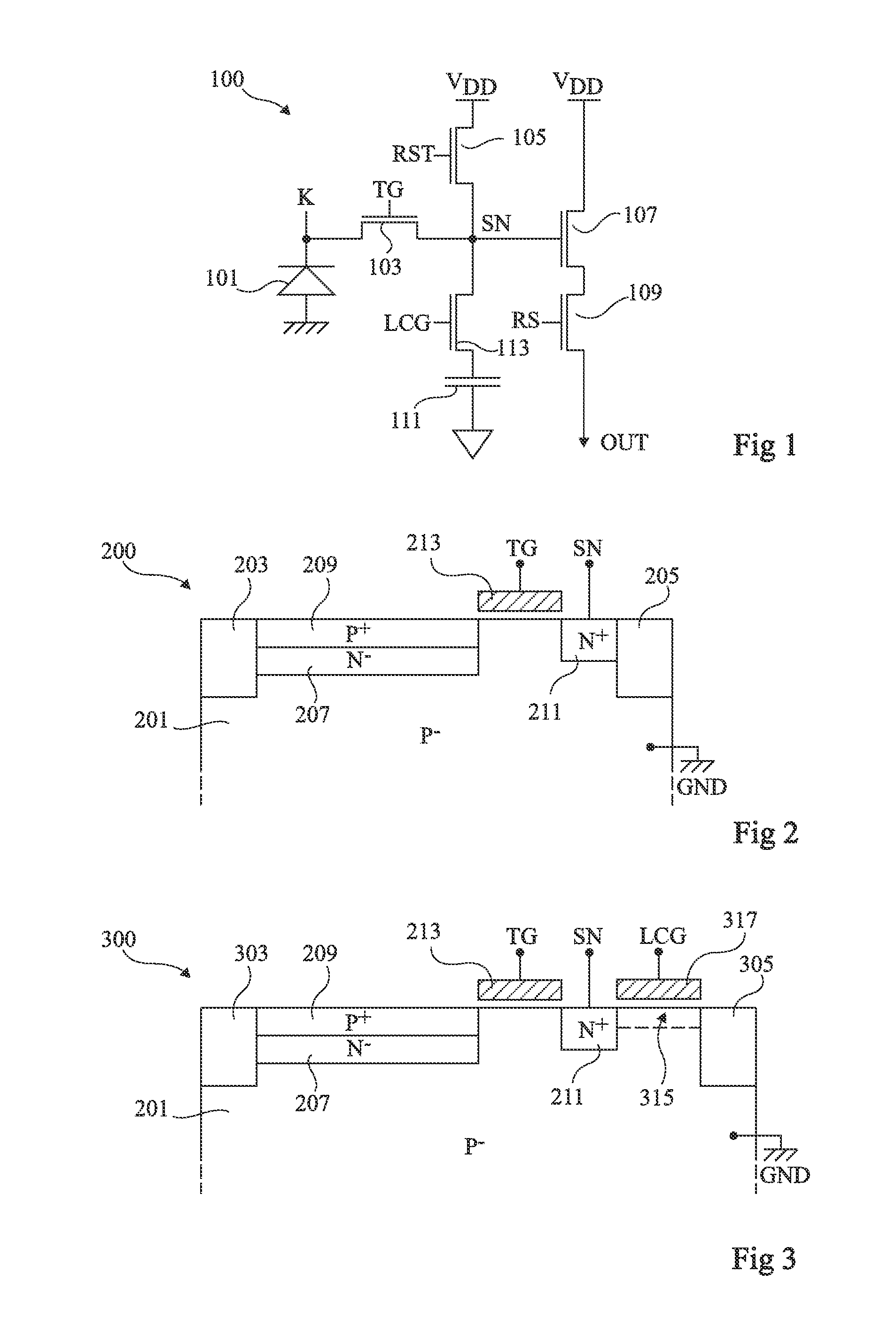
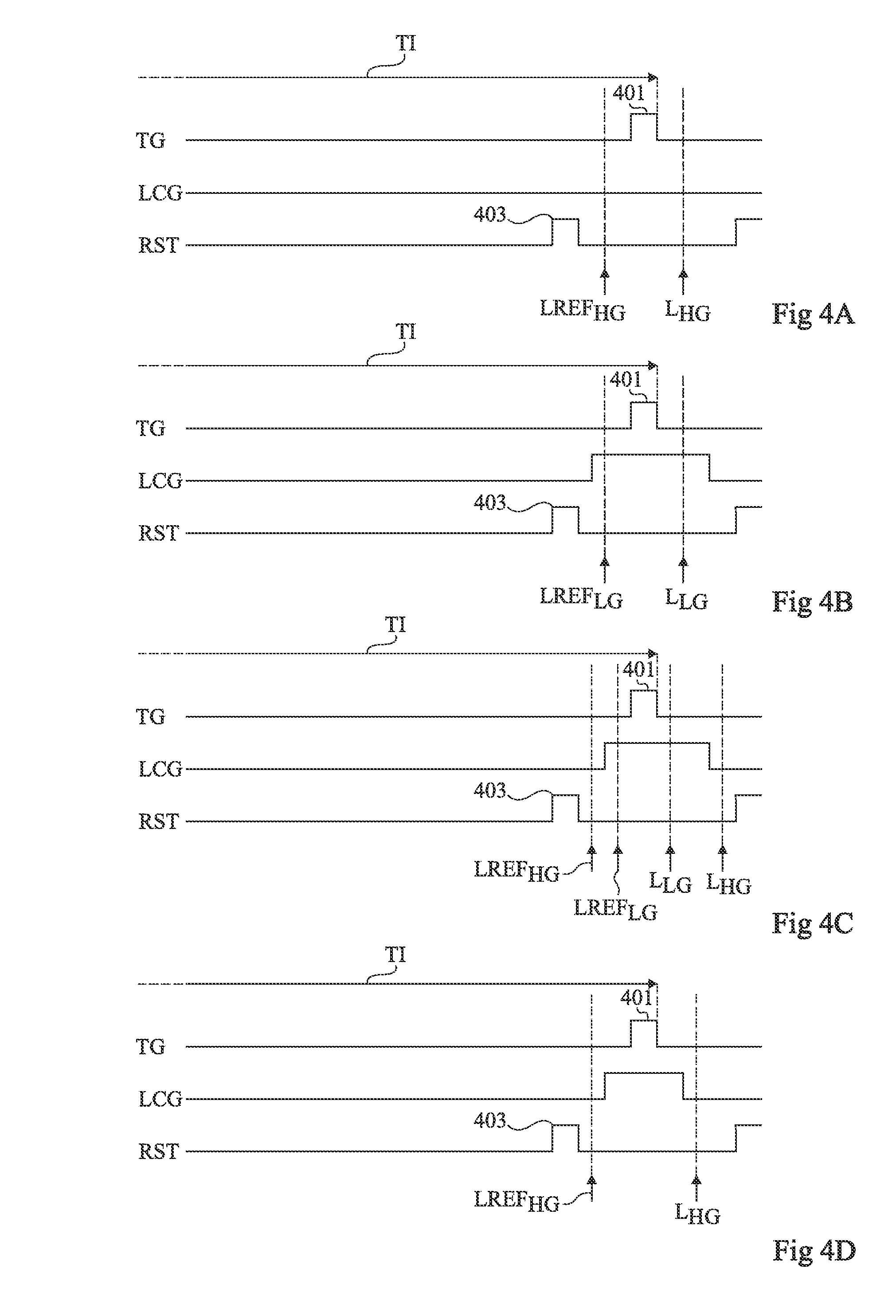
[0024]FIG. 1 illustrates an electric diagram of an example of a pixel 100 having a dual charge-to-voltage conversion gain. Pixel 100 comprises a photodiode 101 having its anode connected to a node or rail of application of a low voltage GND, generally the ground, and having its cathode K, or accumulation node, coupled, via a transfer transistor 103, to a sense node SN. Sense node SN is coupled by a reset ...


PUM


Abstract

An image sensor cell formed inside and on top of a substrate of a first conductivity type, including: a read region of the second conductivity type; and, adjacent to the read region, a storage region of the first conductivity type topped with a first insulated gate electrode. The first electrode is arranged to receive, in a first operating mode, a first voltage causing the inversion of the conductivity type of the storage region, so that the storage region behaves as an extension of the read region, and, in a second operating mode, a second voltage causing no inversion of the storage region.

Description

BACKGROUND[0001]1. Technical Field[0002]The present disclosure relates to image sensors, and more specifically to a CMOS sensor comprising pixels of dual charge-to-voltage conversion gain.[0003]2. Description of the Related Art[0004]Conventionally, a CMOS image sensor includes a plurality of pixels, each having a photodiode used in reverse mode, having its junction capacitance discharged by a photocurrent according to a received light intensity. At the end of a so-called integration period, before and after which the pixel is reset by recharging its photodiode, the photogenerated charges stored in the photodiode are transferred to a capacitive read node of the pixel. The measurement of the illumination level received by the pixel is performed by measuring the read node voltage.[0005]The read node capacitance conditions the pixel sensitivity to illumination level variations. The lower the read node capacitance, the higher the charge-to-voltage conversion factor or gain of the pixel, ...

Claims


Application Information

Patent Timeline
IPC IPC(8): H01L27/146H01L31/103H04N5/378
CPCH01L31/103H01L27/14643H04N5/378H01L27/14612H04N25/75
Inventor ROY, FRANCOIS
Owner STMICROELECTRONICS INT NV
Why Eureka
Eureka Blog
Learn More