Contactless data transmission device, security and/or valuable document including the same and method for manufacturing the contactless data transmission device

a technology of contactless data and transmission device, which is applied in the near field of read/write/interrogation/identification system, instruments, printing, etc., can solve the problems of increasing the cost involved, affecting the use of the device, and the transmission device mentioned above is disadvantageous, etc., to achieve good mechanical properties, reduce costs, and improve the effect of the effect of the transmission devi

Active Publication Date: 2015-01-29
BUNDESDRUCKEREI GMBH
View PDF4 Cites 23 Cited by
  • Summary
  • Abstract
  • Description
  • Claims
  • Application Information

AI Technical Summary

Benefits of technology

[0044]In a further preferred development of the present invention, the electronic component is, in particular, a semiconductor component. The semiconductor component can be formed by an unhoused semiconductor chip (bare die). This allows further cost reductions for manufacture of the contactless data transmission device according to the invention since the chip does not initially have to be mounted in a module. As an alternative, the component can, however, also be a housed component, for example a Surface Mount Device (SMD) or a Chip Scale Package (CSP), or be in one of the following housing forms: DIP, TQFP, MLF, SOTP, SOT, PLCC, QFN, SSOT, BGA, MOB, or other usual housing forms. Furthermore, one can also use a sub-module as a chip carrier based on flexible circuit boards (interposa) made from polyimide, FR4, PC, thin glass. The electronic component has at least two contact points, which are arranged on the contacting side of the component at opposing sides of an edge of the element.
[0045]In a further preferred development of the present invention, the semiconductor chip is mounted on the antenna conductor track according to the flip-chip technique. This technique includes the fact that the chip is mounted (mechanically and electrically connected) at its contact points via contact bumps with the contacting side of the chip being oriented downwards onto the antenna conductor track. To this effect, one uses an anisotropic conductive adhesive typically, which fills the whole space between the contacting side of the chip and the side of the carrier on which the antenna conductor track is located. This adhesive has the property of only creating an electrical contact in those areas in which the contact surface...

Problems solved by technology

The transponders mentioned above do, however, prove to be disadvantageous since the investment required for their manufacture is relatively high.
This requires additional operational steps which increase the costs involved.
The circuit shown in US 2009/0315799 A1 has the disadvantage that the resonance frequency achieved with the antenna arrangement is very high so that tuning...

Method used


Image

  • Contactless data transmission device, security and/or  valuable document including the same and method for  manufacturing the contactless data transmission device
  • Contactless data transmission device, security and/or  valuable document including the same and method for  manufacturing the contactless data transmission device
  • Contactless data transmission device, security and/or  valuable document including the same and method for  manufacturing the contactless data transmission device

Examples


fifth embodiment

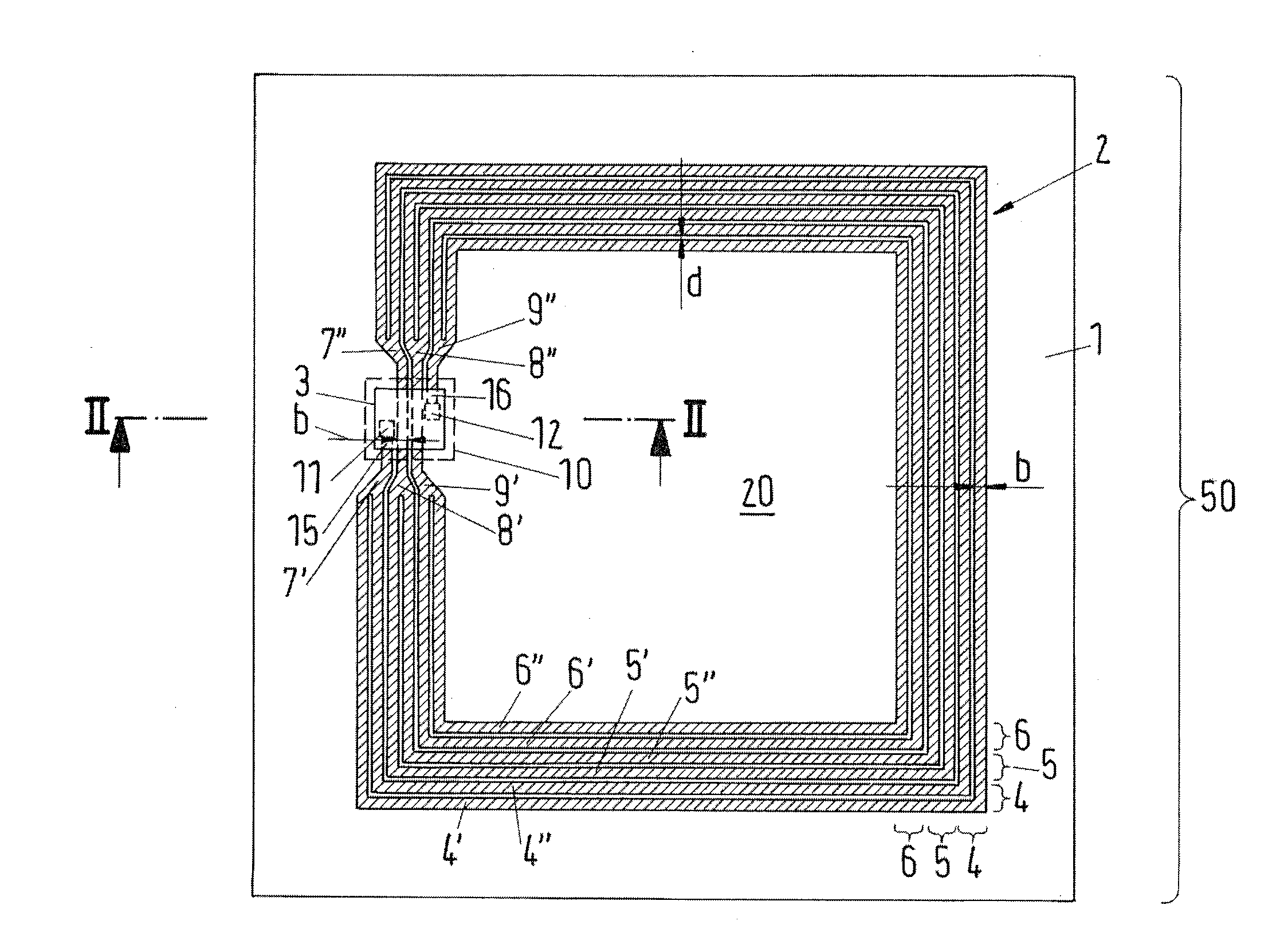
[0091]a data transmission device 50 according to the invention shown in FIG. 6 differs from the one shown in FIG. 3 in that there are additionally provided a plurality (two, three, four or even more) connecting elements 35′, 35″, 35′″, 35″″, 36′, 36″, 36′″, 36″″ (35, 36) between the spiral winding branches 5′, 5″ or 6′, 6″, respectively, or alternatively just one respective connecting element. These connecting elements 35, 36 short circuit the respective spiral winding branches 5′, 5″, 6′, 6″ at the corresponding locations and lead to the situation that the inductance of the antenna conductor track 2 is increased and therefore the resonance frequency of the circuit element is reduced. The resonance frequency can be reduced through increasing the number of connecting elements 35, 36 and through their reduction be increased. The connecting elements 35, 36 can also be provided at other locations than at the locations shown in FIG. 6. The connecting elements 35, 36 have preferably exact...

seventh embodiment

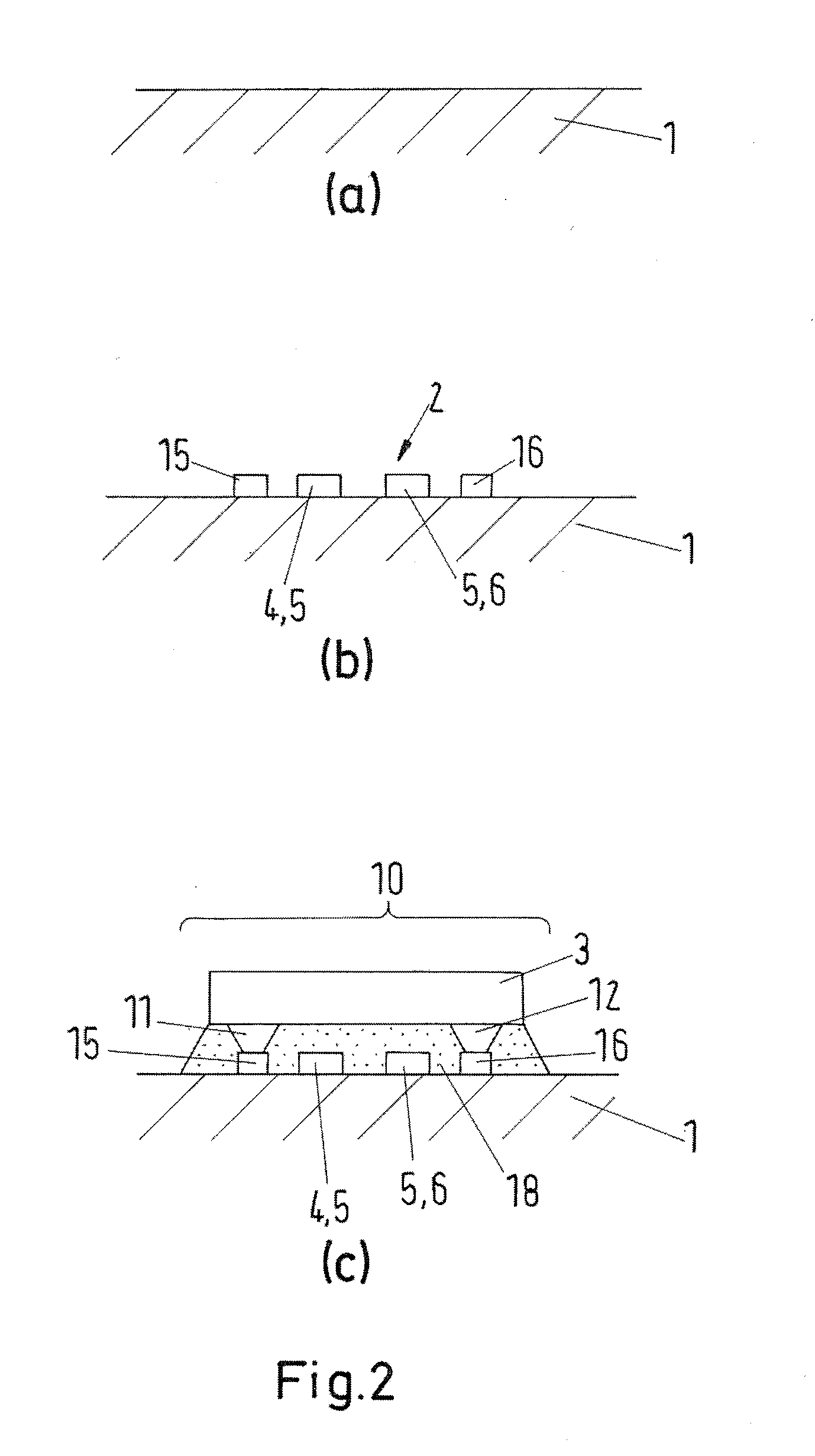
[0095]The seventh embodiment shown in FIG. 9 is presented as a cross-section through the data transmission device 50 from FIG. 3, wherein additionally a material with a high dielectric constant is applied to the mounting side of the carrier 1 after generation of the circuit element and mounting of the chip 3. This material forms a layer 30 whose thickness essentially corresponds to the mounting height of the chip 3. This layer can therefore be used as a compensation layer. The material contains barium titanate to increase the dielectric constant.


PUM

PropertyMeasurementUnit
Electrical conductoraaaaaaaaaa

Abstract

This present invention serves to simplify manufacture of a contactless data transmission device (50). This device (50) has an electrically insulating carrier (1), a circuit element arranged on the carrier (1) made from a continuous antenna conductor track (2) in the form of at least one spiral winding (4, 5, 6) and respectively one terminal contact (15, 16) at the ends thereof as well as an electronic component (3) with at least two contact points (11, 12) electrically connected with the circuit element. The electronic component (3) is placed in a mounting region (10) above the at least one spiral winding (4, 5, 6). The at least two contact points (11, 12) of the component (3) are electrically connected with a respective terminal contact (15, 16) of the antenna conductor track (2). At least one spiral winding (4, 5, 6) is branched outside the mounting region (10) between two respective branching points (7′, 7″; 8′, 8″; 9′, 9″) into at least two spiral winding branches (4′, 4″; 5′, 5″; 6′, 6″). The data transmission device (50) is a component part of a valuable and/or security document (100).

Description

BACKGROUND OF THE INVENTION[0001]1. Field of the Invention[0002]The present invention concerns a contactless data transmission device, a valuable and / or security document which contains a data transmission device of this type, as well as a method for manufacturing the contactless data transmission device.[0003]2. Brief Description of the Related Art[0004]Contactless data transmission devices of this type are known. In order to achieve data storage and / or data processing in a valuable and / or security document, for example, electronic components have been integrated into the document for some time now with which the data can be stored and / or processed. According to the invention, one particularly means semiconductor chips when one refers to electronic components, in particular such chips which are suitable for storage and processing of data. The electronic components can, in particular, be electronic semiconductor circuit elements. The electronic components can particularly include so...

Claims


Application Information

Patent Timeline
IPC IPC(8): G06K19/077H01Q1/22
CPCG06K19/07783H01Q1/2225G06K19/07745G06K19/07754H04B5/0056H04B5/0081H01L2224/16227H01L2224/81191H01L2224/16225H01L2924/07811H01L2924/12044B42D25/305B42D25/455B42D25/46H01L2924/00014Y10T29/49018H01L2924/00H01L2224/0401
Inventor FISCHER, JORGMUTH, OLIVERPAESCHKE, MANFREDTIETKE, MARKUSKLOESER, JOACHIMHOLINSKI, DENISFERBER, ALEXANDERTROLENBERG, STEFAN
Owner BUNDESDRUCKEREI GMBH
Why Eureka
Try Eureka