Method for charged-particle multi-beam exposure

a multi-beam exposure and charged particle technology, applied in the field of charged particle multi-beam exposure, can solve the problems of increasing the number of pixels required to obtain a sufficiently good feature resolution at standard chip size, reducing the efficiency of rasterization, so as to reduce the effect of heating

Active Publication Date: 2015-01-29
IMS NANOFABTION
View PDF6 Cites 41 Cited by
  • Summary
  • Abstract
  • Description
  • Claims
  • Application Information

AI Technical Summary

Benefits of technology

[0022]This solution according to many embodiments of the invention modifies the “trotting mode” method in order to make it more flexible and to allow an additional redundancy scheme in order to limit the influence of local defects on or within the PD device. Furthermore, many embodiments of the invention allow for an improved tolerance against imaging errors and aberrations of the optical system. This tolerance is due to the effect that the same region on the target is exposed by beamlets originating from different regions in the PD device, thus leveling out the influence of any errors over the imaged region on the target.
[0029]One suitable way to distribute the stripes is that for each stripe, a boundary of said stripe having an orientation parallel to said main direction falls within a central region of a stripe of a different pass. This arrangement helps to level out potential imaging errors over the pattern image formed in the exposure on the target.
[0032]Furthermore, the stripes of at least one of the passes may overlap. In such a case, the range of overlap of two stripes of the same pass is suitable such that nominal positions of pattern pixels of one of the two stripes are overlapping with nominal positions of corresponding pattern pixels of the other of the two stripes. In this case the pattern pixels falling into the overlap range are exposed in at most one of the two overlapping stripes, or more generally, in the two overlapping stripes in a complementary manner with regard to the pattern to be imposed. This method allows a smooth transition between patterns imaged by the adjacent stripes, so as to once more alleviate the effect of imaging deviations at the edge of stripes.
[0037]A further aspect of many embodiments of the invention further reduces the effects of heating or resist charging during the exposure of a pattern on a target by applying a special ordering of the stripes: In particular, according to this aspect the stripes of each pass are distributed into at least two groups of spatially adjacent stripes, and the stripes are written either in a time sequence (a) wherein either each stripe is followed by a non-adjacent stripe of a different group, or in a time sequence (b) wherein the stripes are written in groups of stripes according to the order of the groups, with each group of stripes being followed by a non-adjacent different group.

Problems solved by technology

The number of pixels required to obtain a sufficiently good feature resolution at standard chip sizes is quite high and remains a challenging task.
Therefore, the storage of the complete rasterized image data is not feasible.
The particle optical system is generally non-ideal, which means that the system has imaging defects, in particular image distortions and blur variations, which additionally may vary over time, temperature and image position.
A change of one of these parameters is generally not possible without altering the layout of the blanking plate.
The filing of the present application was triggered by the observation that the performance of a multibeam writing system is often limited by the data rate that can be processed and transferred into the PD device.

Method used


Image

  • Method for charged-particle multi-beam exposure
  • Method for charged-particle multi-beam exposure
  • Method for charged-particle multi-beam exposure

Examples


Embodiment Construction

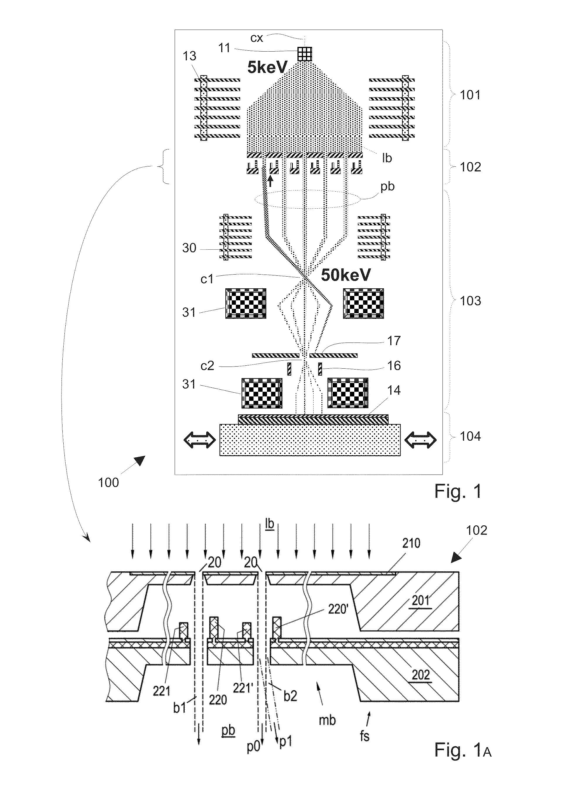
[0065]One embodiment of the invention discussed in the following is a development from the particle-beam exposure apparatus of PML2 and eMET type with a pattern definition (PD) system as disclosed in U.S. Pat. No. 6,768,125 and U.S. Pat. No. 7,781,748 of the applicant, and with a large-reduction projecting system. In the following, first the technical background of the apparatus is discussed—as far as relevant to many embodiments of the invention—, then certain embodiments of the invention is presented in detail.

[0066]It should be appreciated that the invention is not restricted to the following embodiments or the particular layout of the PD system, which merely represent one of the possible applications of the invention; embodiments of the invention are suitable for other types of processing systems that use a multi-beam setup for exposure of a target.

Charged-Particle Multi-Beam System

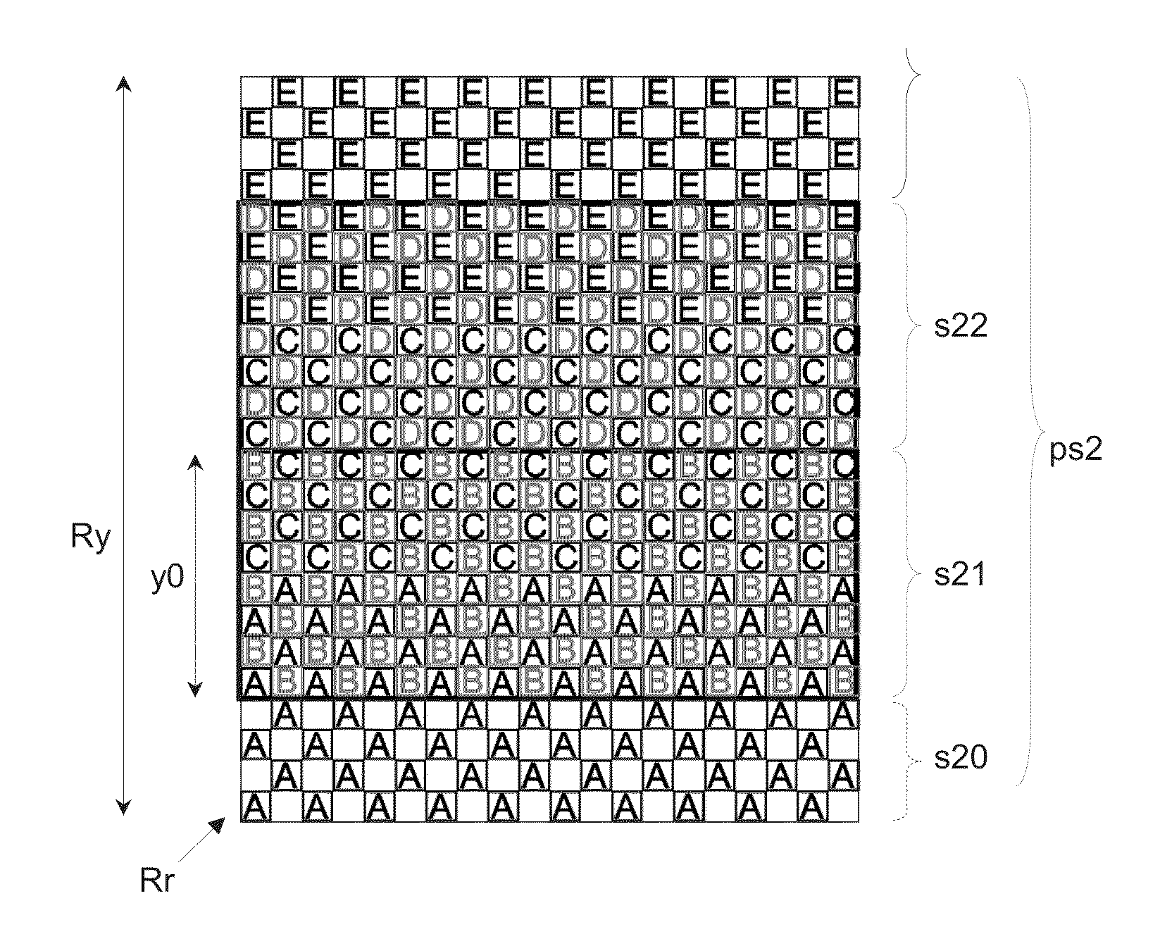
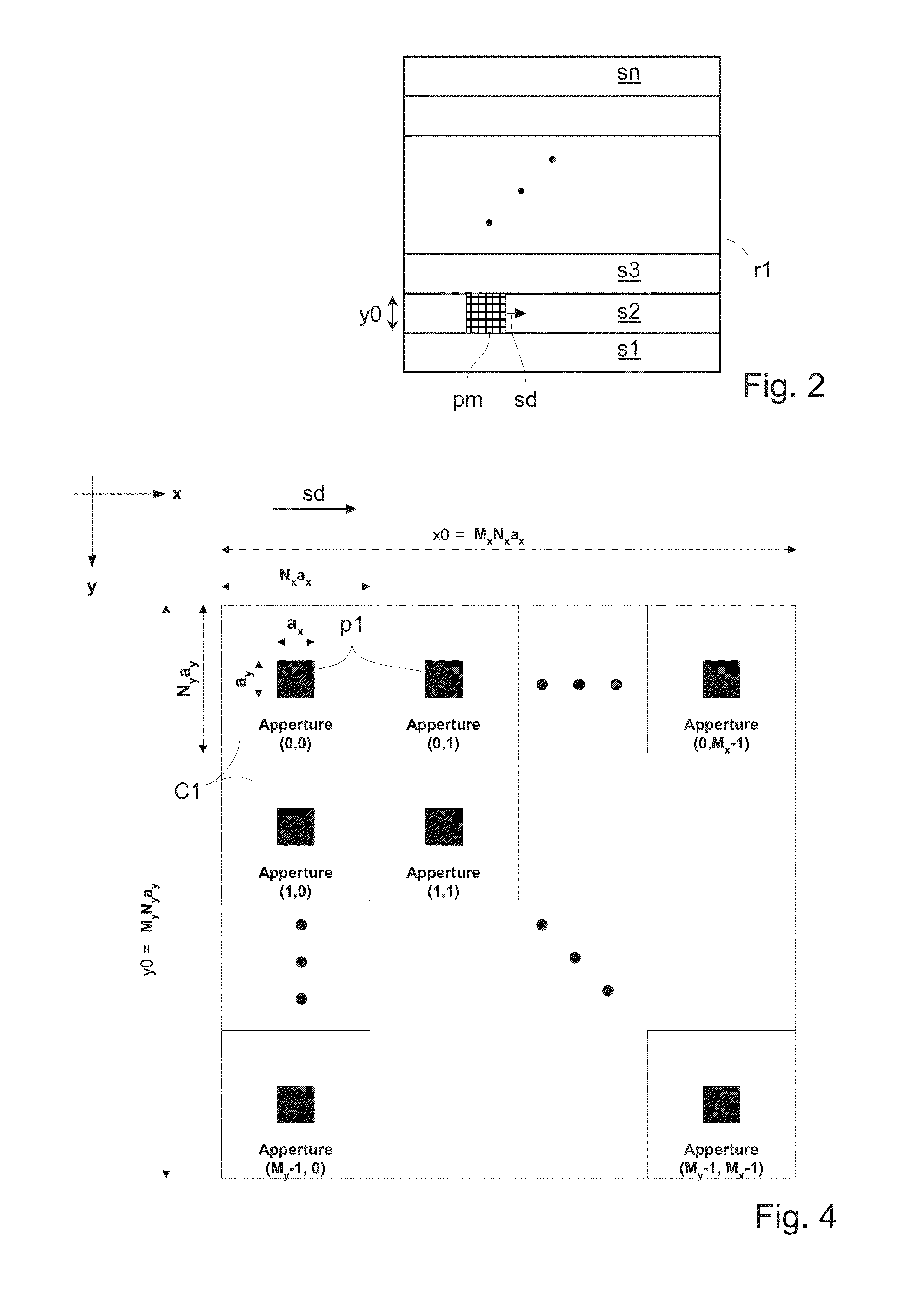
[0067]A schematic overview of a charged-particle multi-beam mask exposure tool (mask writer) emplo...


PUM


Abstract

To irradiate a target with a beam of energetic radiation formed by electrically charged particles, the beam is formed and imaged onto a target, where it generates a pattern image composed of pixels. The pattern image is moved along a path on the target over a region to be exposed, and this movement defines a number of stripes covering said region in sequential exposures and having respective widths. The number of stripes is written in at least two subsequent passes such that for each pass, the widths of the stripes of one pass combine into a cover of the total width of the region to be exposed; and each pass is associated with one of a number of partial grids of pattern pixels which are exposable during the respective pass. The mutually different partial grids combine to the complete plurality of pattern pixels which compose the region to be exposed.

Description

CROSS-REFERENCE TO RELATED APPLICATIONS[0001]The present application claims priority to European Application No. 13178066.0 filed Jul. 25, 2013, and also claims priority to European Application No. 13194388.8 filed Nov. 26, 2013, the disclosures of which are herein incorporated by reference in their entirety.FIELD OF THE INVENTION AND DESCRIPTION OF PRIOR ART[0002]The present invention generally relates to a method for forming a pattern on a surface of a target by means of a beam formed of electrically charged particles. More in detail, the invention generally relates to a method for irradiating a target with a beam of energetic radiation formed by electrically charged particles, which comprises the steps of[0003]providing a pattern definition means having a plurality of apertures transparent to said radiation,[0004]illuminating said pattern definition means by means of an illuminating wide beam, which traverses the pattern definition means through said apertures, thus forming a pat...

Claims


Application Information

Patent Timeline
Patent Type & Authority Applications(United States)
IPC IPC(8): H01J37/302H01J37/317
CPCH01J37/3026H01J2237/31774H01J2237/31764H01J37/3175H01J37/3177H01J2237/31754H01J2237/31766
Inventor PLATZGUMMER, ELMAR
Owner IMS NANOFABTION
Why Eureka
Try Eureka