Organic light emitting diode, manufacturing method for organic light emitting diode, image display device, and illumination device

a light emitting diode and manufacturing method technology, applied in the direction of solid-state devices, semiconductor devices, thermoelectric devices, etc., can solve the problems of low light extraction efficiency, and relationship between, and achieve excellent effect and high light extraction efficiency

Active Publication Date: 2015-02-05
OJI HLDG CORP
View PDF1 Cites 19 Cited by
  • Summary
  • Abstract
  • Description
  • Claims
  • Application Information

AI Technical Summary

Benefits of technology

[0075]Since the present invention is constituted as described above, it exerts an excellent effect that high light extraction efficiency can be obtained, light in a narrow bandwidth having a certain degree of broadness in a region from visible light to near infrared can be extracted, and there is no risk that the extraction wavelength is deviated from the target light emission wavelength by a slight change of the fine uneven structure.

Problems solved by technology

Features of such an organic light emitting diode are advantages that less view angle dependency, less power consumption, it can be fabricated extremely thin, and, on the other hand, a problem that light extraction efficiency being efficiency of extracting light from the light emitting layer to the outside is low.
Further, since a distance between the light emitting layer and the cathode formed by metal is close, a part of near field light from the light emitting layer was converted into surface plasmon on the surface of the cathode and lost, by which light extraction efficiency was reduced.
However, the relationship between the pitch of the periodic fine uneven structure and the extraction wavelength has not been known regarding the cathode top emission-type element.
Actually, since the cathode top emission-type element is used regarding an active matrix type display using the organic light emitting diode, the fact that the most suitable fine uneven structure for increasing light extraction efficiency had been unknown was significantly inconvenient.
Further, regarding light extraction of the organic light emitting diode, an important problem other than the one described above is known.
Specifically, in the case of implementing the fine uneven structure made of a lattice having a single periodic structure into an element in order to improve the light extraction efficiency of a monochromatic organic light emitting diode, regardless of a type of the layer constitution of the organic light emitting diode, there was a problem that effect of extraction efficiency improvement had not obtained unless matching between the pitch of the fine uneven structure and the extraction wavelength had been accurate.
This problem applies to all of the bottom emission-type element, the anode top emission-type element, and the cathode top emission-type element.
However, there was a problem that the light extraction efficiency of the fine uneven structure for the white organic light emitting diode had been worse than the light extraction efficiency of the fine uneven structure for the monochromatic organic light emitting diode in the case where a light emission wavelength was limited to a certain narrow bandwidth.
However on the other hand, the fine uneven structure having high light extraction efficiency has a narrow allowable range of a deviation of period, so there was a problem of risk that the extraction wavelength is deviated from a target light emission wavelength when the fine uneven structure only slightly changed.
Therefore, in the case of aiming at obtaining broadband light such as the case where the light extraction efficiency of white light needs to be increased, it has been pointed out obtaining desired light was difficult on the organic light emitting diode substrate having a two-dimensional lattice structure whose period of the uneven structure was constant.
However, an attempt of obtaining power spectrum intensity by simply increasing the height of the uneven structure is not preferable because it causes a new problem that surface plasmon tends to be localized and a short circuit in an element easily occurs.
In other words, according to the organic light emitting diode having the uneven structure with the irregular pitch, although an organic light emitting diode having extraction efficiency of electromagnetic wave in an arbitrary broadband wavelength region from the visible light to near infrared region can be realized and there is no possibility that the extraction wavelength is deviated from a target light emission wavelength when the fine uneven structure only slightly changed, it caused a new problem that the intensity of light to be extracted becomes weak.

Method used


Image

  • Organic light emitting diode, manufacturing method for organic light emitting diode, image display device, and illumination device
  • Organic light emitting diode, manufacturing method for organic light emitting diode, image display device, and illumination device
  • Organic light emitting diode, manufacturing method for organic light emitting diode, image display device, and illumination device

Examples


first embodiment

(1) First Embodiment

[0094]Hereinafter, referring to the accompanying drawings, the organic light emitting diode by the first embodiment of the present invention will be explained in detail.

[0095]Now in the explanation below, as long as the present invention is used, a structure and a method of a target organic light emitting diode are not necessarily limited.

(1-1) Constitution of the Organic Light Emitting Diode by the First Embodiment

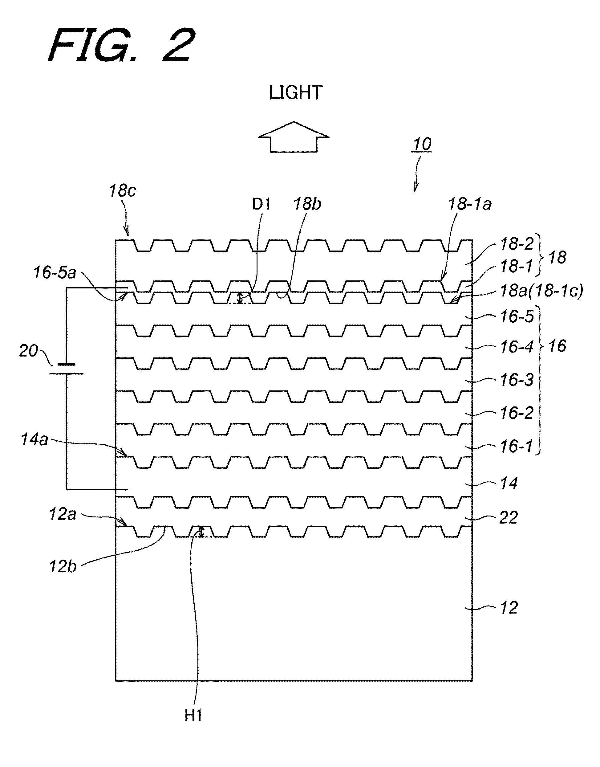
[0096]Herein, FIG. 2 shows a schematic constitution explanatory view showing the organic light emitting diode by the first embodiment of the present invention.

[0097]The organic light emitting diode 10 shown in FIG. 2 is a monochromatic organic light emitting diode of a type generally referred to as a top emission-type with a cathode at the top, and a reflective layer 22, an anode conductive layer 14, an organic EL layer 16, and a cathode conductive layer 18 are sequentially stacked on a substrate 12.

[0098]Then, the diode is designed that voltage can be...

second embodiment

(2) Second Embodiment

[0320]Hereinafter, referring to the accompanying drawings, an example of a second embodiment of the organic light emitting diode according to the present invention will be explained in detail.

[0321]Now in this embodiment as well, as long as the present invention is used, a structure and a method of a target organic light emitting diode are not necessarily limited in the explanation below.

(2-1) Constitution of the Organic Light Emitting Diode by the Second Embodiment

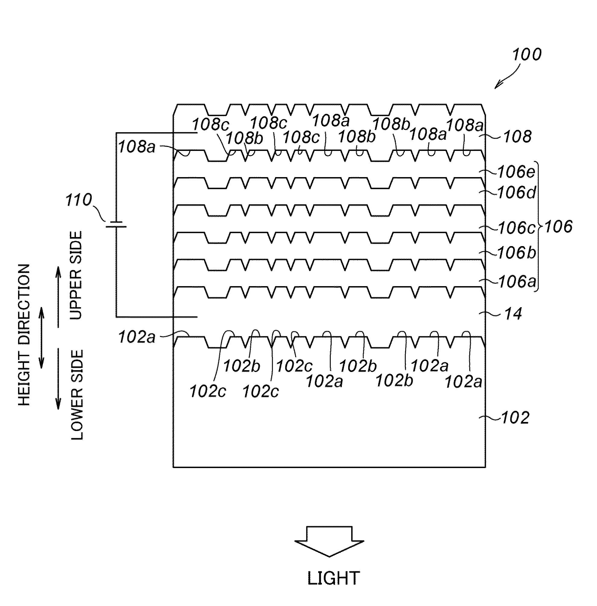
[0322]Firstly, FIG. 8 shows a schematic constitution cross-sectional explanatory view showing the second embodiment of the organic light emitting diode according to the present invention.

[0323]Now, in the explanation regarding the organic light emitting diode 100 according to the present invention shown in FIG. 8, for convenience of explanation, a surface on an upper side in a height direction of each layer constituting the monochromatic organic light emitting diode 100 is appropriately referred to as...


PUM


Abstract

The present invention provides an organic light emitting diode substrate configured so that the light extraction efficiency of a single color organic light emitting diode element made from one type of light emitting material is high, so that there is no risk of an extraction wavelength deviating from a target light emission wavelength due to slight variations in a fine uneven structure, and so as to enable extraction of a narrow bandwidth of light, from visible light, that has any central wavelength within the near infrared band and that has a degree of broadness. Also provided are an organic light emitting diode, a manufacturing method for the organic light emitting diode substrate, a manufacturing method for the organic light emitting diode, an image display device, and an illumination device. The organic light emitting diode, which is a top emission-type, is configured so that at least the following are laminated on the substrate: a reflective layer comprising a metal material; an anode conductive layer comprising a transparent conductive material; an organic EL layer having a light emitting layer which contains an organic light emitting material; and a cathode conductive layer in which a semi-transmissive metal layer and a transparent conductive layer comprising a transparent conductive material are laminated. On the surface of the semi-transmissive metal layer that is in contact with the transparent conducive layer side, a two-dimensional lattice structure is formed in which a plurality of protrusions are arranged periodically and two-dimensionally. If in the surface the real part of propagation constant of a surface Plasmon expressed by complex numbers is k, a distance between centers (P), which is the distance between centers (P) of adjacent protrusions from among the protrusions formed on the surface, is set to be a value within the range of formula (1). When forming a triangular lattice structure as the two-dimensional lattice structure, P0 in formula (1) satisfies formula (2), and when forming a rectangular lattice structure as the two-dimensional lattice structure, P0 satisfies formula (3).[MathematicalFormula1]0.8P0≤P≤1.2P0(1)[MathematicalFormula2]P0=4π√3k(2)[MathematicalFormula3]P0=2πk(3)

Description

TECHNICAL FIELD[0001]The present invention relates to an organic light emitting diode substrate, an organic light emitting diode, a manufacturing method for an organic light emitting diode substrate, a manufacturing method for an organic light emitting diode, an image display device and an illumination device. More particularly, the invention relates to an organic light emitting diode substrate which emits light by injection and recombination of electrons and holes and has an uneven structure, an organic light emitting diode, a manufacturing method for an organic light emitting diode substrate, a manufacturing method for an organic light emitting diode, an image display device and an illumination device.BACKGROUND TECHNOLOGY[0002]An organic light emitting diode is a light emitting element utilizing organic electro-luminescence (hereinafter, referred to as organic EL (Organic Electro-Luminescence)), and generally has a constitution that an organic EL layer including a light emitting ...

Claims


Application Information

Patent Timeline
Patent Type & Authority Applications(United States)
IPC IPC(8): H01L51/52H01L51/56H01L51/50
CPCH01L51/5271H01L51/56H01L51/5012H10K50/818H10K50/828H10K50/858H10K2102/3026H10K2102/331H10K50/85H10K50/805H10K50/11H10K50/856H10K71/00
Inventor SHINOTSUKA, KEIOKAMOTO, TAKAYUKIKAWAMUKAI, ETSUKO
Owner OJI HLDG CORP
Why Eureka
Try Eureka