Chip-on-wafer bonding method and bonding device, and structure comprising chip and wafer
What is AI technical title?
AI technical title is built by Patsnap AI team. It summarizes the technical point description of the patent document.
a chip-on-wafer and bonding surface technology, applied in auxillary welding devices, semiconductor/solid-state device testing/measurement, semiconductor/solid-state device details, etc., can solve the problem of increasing the difficulty of removal flux, increasing the packaging density of chip-mounting, and increasing the minuteness of the microstructure of the bond surface. , to achieve the effect of good electroconductivity, high mechanical strength and high production efficiency
Active Publication Date: 2015-02-19
BONDTECH
View PDF1 Cites 47 Cited by
Summary
Abstract
Description
Claims
Application Information
AI Technical Summary
This helps you quickly interpret patents by identifying the three key elements:
Problems solved by technology
Method used
Benefits of technology
Benefits of technology
The present invention provides a method for bonding chips to a substrate with strong and clean bonds. By using treated bond surfaces, water and other substances are removed, resulting in a better electroconductivity and higher mechanical strength. The method also allows for efficient production with a higher packaging density.
Problems solved by technology
However, the removal of the flux tends to be increased in difficulty with an increase in the packaging density in chip-mounting and a rise in the minuteness of microstructures of the bond surface.
Method used
Image
Click on the blue label to locate the original text in one second.
Reading with bidirectional positioning of images and text.
Examples
first embodiment
1.1 First Embodiment
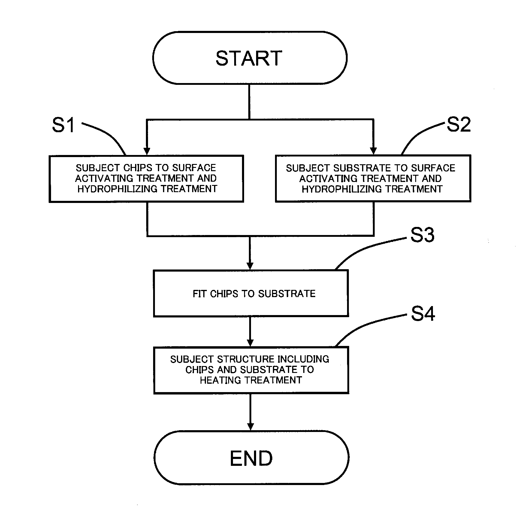
[0098]FIG. 1 is a flowchart showing a method according to a first embodiment of the present invention for bonding chips to a substrate.
[0099]In step S1, surfaces of plural chips to be bonded to a substrate (hereinafter referred to as chip-side-bond-surfaces) are subjected to surface activating treatment and hydrophilizing treatment. The chip-side-bond-surfaces each include one or more regions made of a metal (hereinafter referred to as metal region(s)).
[0100]In step S2, about the substrate to which the chip-side-bond-surfaces are to be bonded, its surface regions corresponding to the respective chips (hereinafter referred to as bond portions) are wholly subjected to surface activating treatment and hydrophilizing treatment.
[0101]Herein, a description is made about each of the surface activating treatments in the present invention.
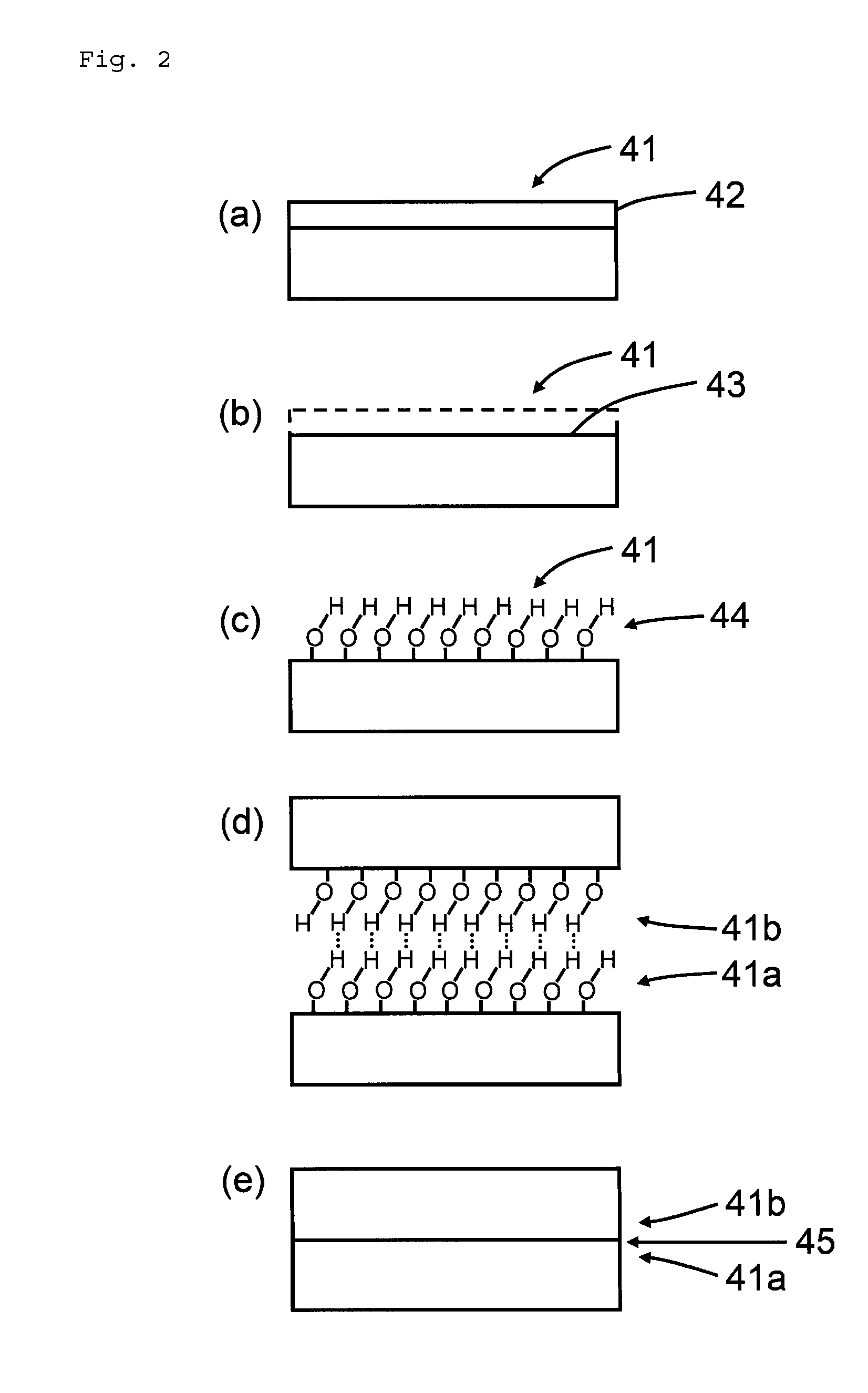
[0102]A surface layer 42 containing respective oxides of various substances, pollutants (impurities) such as an adhering organic substa...
second embodiment
1.2 Second Embodiment
[0237]FIG. 10 is a flowchart showing a method for bonding chips in a multilayered form onto a substrate according to a second embodiment. A processing from step S11 to S13 for fitting chips of a first layer, out of these chips, onto a substrate is identical with step S1 to S3 in the first embodiment. Thus, any description thereabout is omitted herein.
[0238]In the first embodiment, chips corresponding to a single layer are fitted onto a substrate. However, in the second embodiment, chips corresponding to plural layers are fitted onto a substrate. In this point, these embodiments are different from each other. In the second embodiment, the chips in the multilayered form are fitted onto the substrate; thus, the chips laminated into a multilayered form each have a structure having a first bond surface corresponding to any one of the chip-side-bond-surfaces in the first embodiment, and a second bond surface positioned on the rear side of the first bond surface.
[0239]...
modified examples
[0312]In conventional bonding units, their moiety corresponding to the bonding constitution 33 can be shifted in the horizontal direction or the in-plane direction (XY directions) parallel to the front surface of a substrate along a beam of a cantilever structure supported in the horizontal direction inside each of the bonding units. However, the cantilever structure is low in rigidity, so that the cantilever is bent in the Z direction when force is applied thereto at the time of fitting any chip. Thus, when the chip and the substrate contact each other, force applicable thereto is very much limited. Usually, only force of at most about 2 to 3 kgf (kilogram force), i.e., about 20 to 30 N can be applied. In conventional NCP-bonding or bump-solider-bonding methods, chips are merely pre-bonded at one time with resin or flux, and thus a pressuring force of 20 to 30 N is sufficient. Even when solder-bonding is attained in the spot, a large pressuring force is unnecessary since solder is ...
PUM
Property
Measurement
Unit
temperature
aaaaa
aaaaa
pressure
aaaaa
aaaaa
pressure
aaaaa
aaaaa
Abstract
[Problem] Provided is a technique for bonding chips efficiently onto a wafer to establish an electrical connection and raise mechanical strength between the chips and the wafer or between the chips that are chips laminated onto each other in the state that resin and other undesired residues do not remain on a bond interface therebetween.[Solution] A method for bonding plural chips each having a chip-side-bond-surface having metal regions to a substrate having plural bond portions has the step (S1) of subjecting the metal regions of the chip-side-bond-surface to surface activating treatment and hydrophilizing treatment; the step (S2) of subjecting the bond portions of the substrate to surface activating treatment and hydrophilizing treatment; the step (S3) of fitting the chips subjected to the surface activating treatment and the hydrophilizing treatment onto the corresponding bond portions of the substrate subjected to the surface activating treatment and the hydrophilizing treatment to bring the metal regions of the chips into contact with the bond portions of the substrate; and the step (S4) of heating the resultant structure, which includes the substrate, and the chips fitted onto the substrate.
Description
TECHNICAL FIELD[0001]The present invention relates to a chip-on-wafer (COW) bonding method and bonding device for mounting chips onto a wafer, and a structure including a wafer and chips bonded onto the wafer.BACKGROUND ART[0002]In the electronic field, a higher packaging density has been desired for mounting electronic devices. Thus, attention has been paid to a technique of bonding already-packaged semiconductor integrated circuits (chips) onto a wafer (substrate) in a flip chip mounting manner. Chips have metal regions in a bump (projection) form or plate form. Electrical connection can be established through the metal regions between the chips and a wafer; or, in the case of laminating the chips three-dimensionally, between the laminated chips. In order to raise the mechanical strength of anyone of the chips, the chip may have a moiety to be bonded to the wafer or to different one of the chips. The moiety may be formed as one or more metal regions. By use of the metal region(s) ...
Claims
Application Information
Patent Timeline
Application Date:The date an application was filed.
Publication Date:The date a patent or application was officially published.
First Publication Date:The earliest publication date of a patent with the same application number.
Issue Date:Publication date of the patent grant document.
PCT Entry Date:The Entry date of PCT National Phase.
Estimated Expiry Date:The statutory expiry date of a patent right according to the Patent Law, and it is the longest term of protection that the patent right can achieve without the termination of the patent right due to other reasons(Term extension factor has been taken into account ).
Invalid Date:Actual expiry date is based on effective date or publication date of legal transaction data of invalid patent.
Patent Type & AuthorityApplications(United States)

