Boron ionization for aluminum oxide etch enhancement

Inactive Publication Date: 2015-03-19
APPLIED MATERIALS INC
View PDF1 Cites 155 Cited by
  • Summary
  • Abstract
  • Description
  • Claims
  • Application Information

AI Technical Summary

Problems solved by technology

Conventional preclean chambers and processes often do not uniformly clean the surface of the every smaller features being fabricated on a substrate.
Failure to properly clean these features may result in void formation or increased electrical resistance between the surface features.
Although the sputtering processes alone may be effective at rem

Method used


Image

  • Boron ionization for aluminum oxide etch enhancement
  • Boron ionization for aluminum oxide etch enhancement
  • Boron ionization for aluminum oxide etch enhancement

Examples


Embodiment Construction

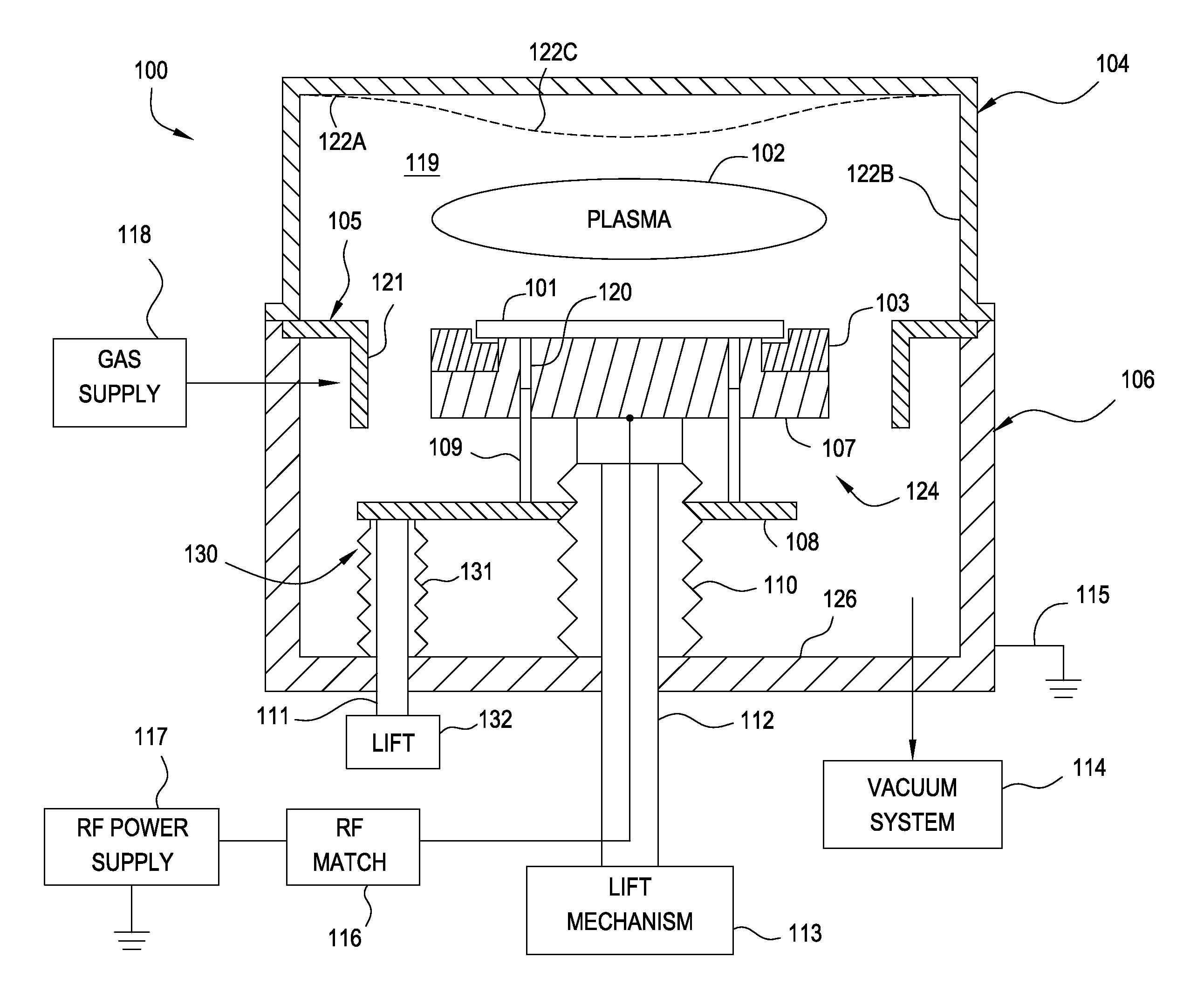
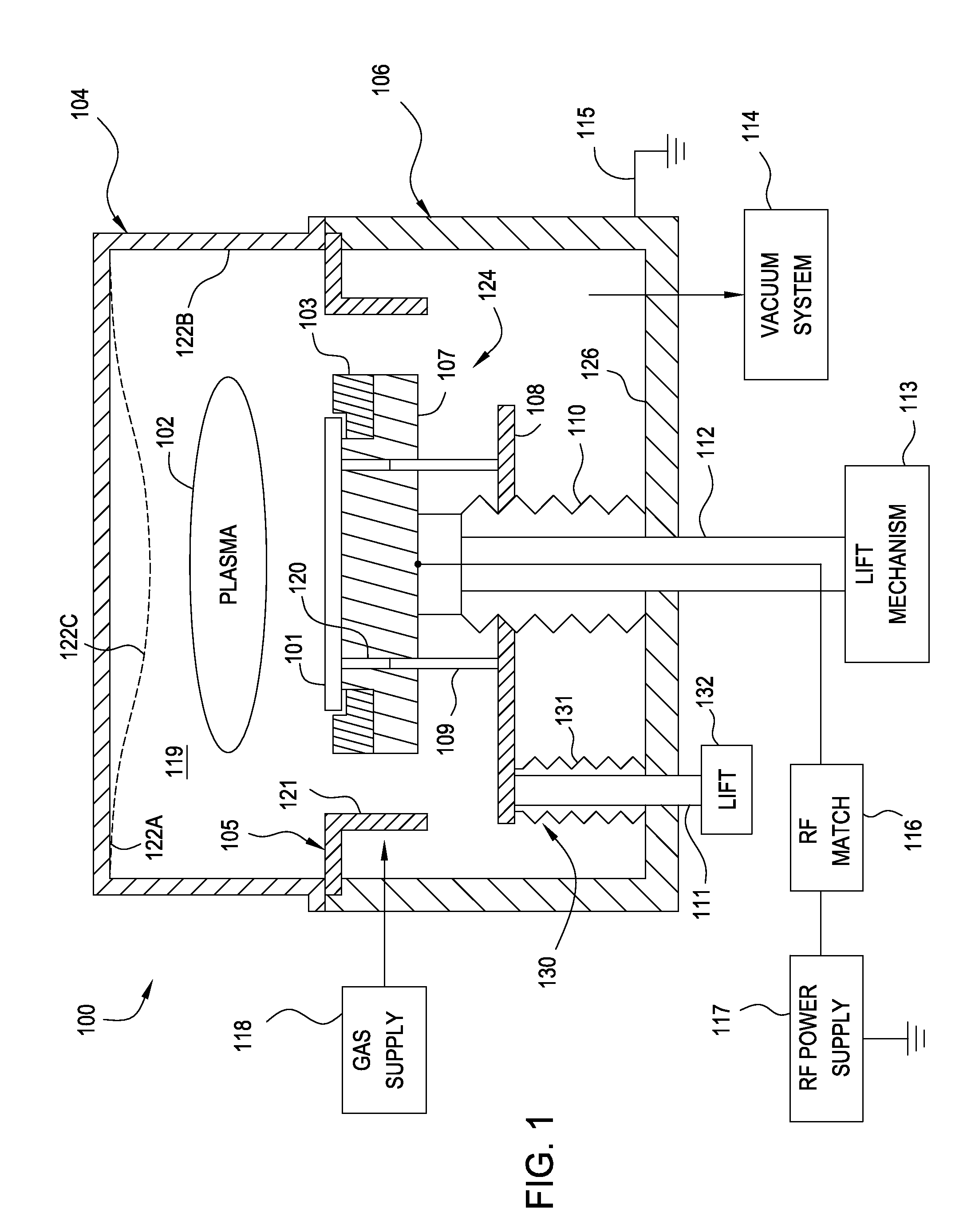
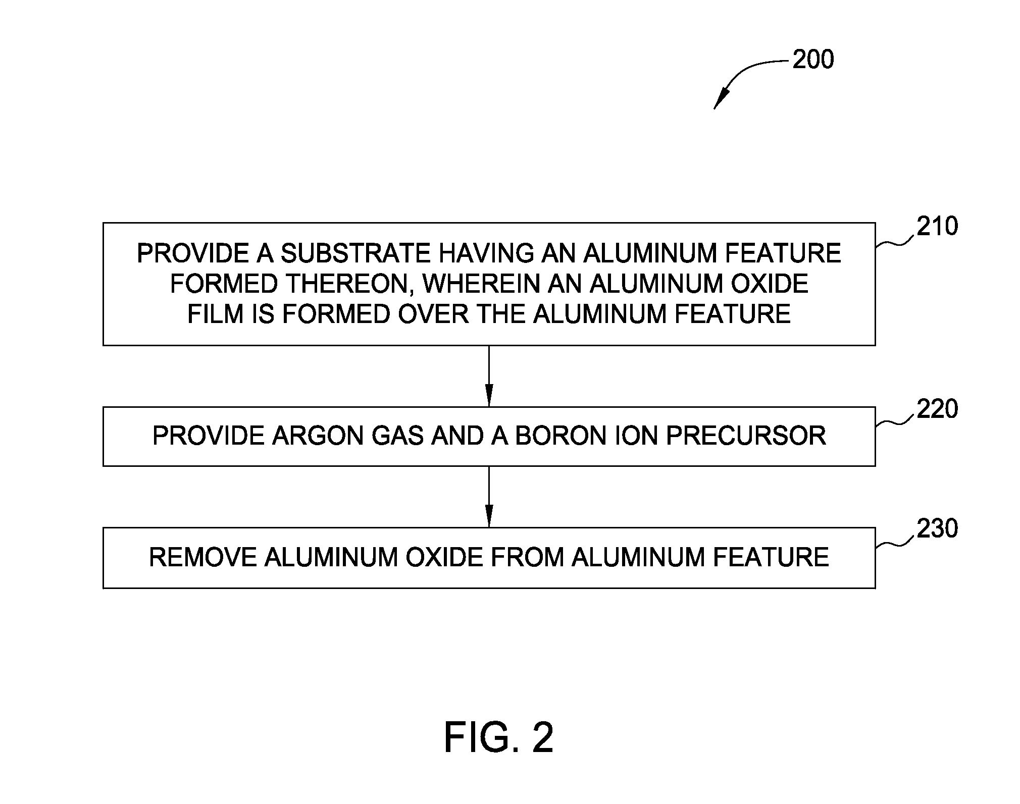
[0017]Embodiments described herein generally provide a method for performing a semiconductor precleaning process. More specifically, embodiments provided herein relate to boron ionization for aluminum oxide etch enhancement. A process for removing native oxide from aluminum may utilize ionized boron alone or in combination with a halogen plasma. The ionized boron may provide improved aluminum oxide etching properties while being highly selective for native oxides more generally.

[0018]FIG. 1 is a cross-sectional schematic view of a sputter etch process chamber according to one embodiment described herein. In another embodiment, other types of plasma processing chambers may be used to practice the embodiments described herein. A chamber 100 may include a chamber body 106 covered by a dome 104 having a top interior surface 122A and sidewall interior surfaces 122B which may enclose a processing volume 119. The dome 104 may be designed to have a top interior surface 122C so that a centra...


PUM

PropertyMeasurementUnit
Temperatureaaaaaaaaaa
Timeaaaaaaaaaa

Abstract

Embodiments described herein generally provide a method for performing a semiconductor precleaning process. More specifically, embodiments provided herein relate to boron ionization for aluminum oxide etch enhancement. A process for removing native oxide from aluminum may utilize ionized boron alone or in combination with a halogen plasma. The ionized boron may provide improved aluminum oxide etching properties while being highly selective for native oxides more generally.

Description

BACKGROUND OF THE INVENTION[0001]1. Field of the Invention[0002]Embodiments of the present invention generally relate to substrate processing systems and chambers used to process semiconductor wafers, solar panels, and flat panel displays and, in particular, to depositing electrically conductive pasting material in a plasma processing chamber.[0003]2. Description of the Related Art[0004]To help ensure semiconductor device integrity and performance, a semiconductor substrate is often cleaned prior to depositing a film on the substrate to remove contaminants and native oxides which may reside on the substrate surface. Conventional preclean processes typically include a sputter etch process to remove the contaminants and expose the native oxides. The native oxides may then be removed by additional sputter etching and / or reactive etching which uses a reduction reaction.[0005]During chip packaging, metal layers are used for connecting solder material to bond pads that are electrically co...

Claims


Application Information

Patent Timeline
IPC IPC(8): C23F4/00H01J37/32
CPCC23F4/00H01J2237/334H01J37/32009C23G5/00H01L21/02068
Inventor WU, KAIYU, SANG HOPARK, KIE JINMORI, GLEN T.COLLINS, JOSHUA
Owner APPLIED MATERIALS INC
Why Eureka
Try Eureka