

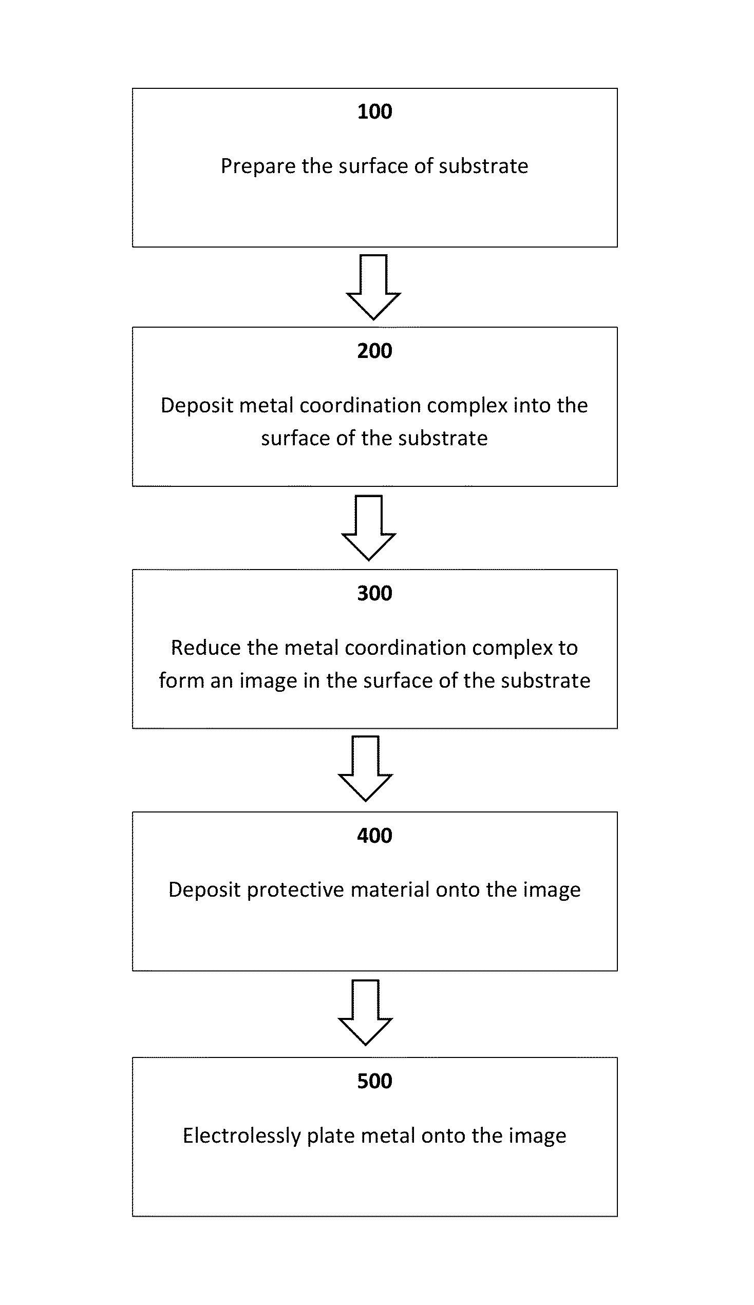
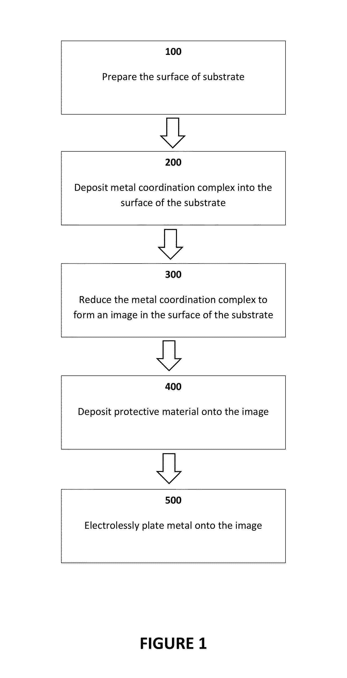
Method of forming a conductive image using high speed electroless plating
a technology of electroless plating and conductive images, which is applied in the direction of liquid/solution decomposition chemical coating, coating, printed circuit manufacturing, etc., can solve the problems of low speed of metal plating film formation, difficult to obtain a high adhesion plating film, and deterioration of devices. , to achieve the effect of high speed and efficacy
- Summary
- Abstract
- Description
- Claims
- Application Information
AI Technical Summary
Benefits of technology
Problems solved by technology
Method used
Image

Examples
example
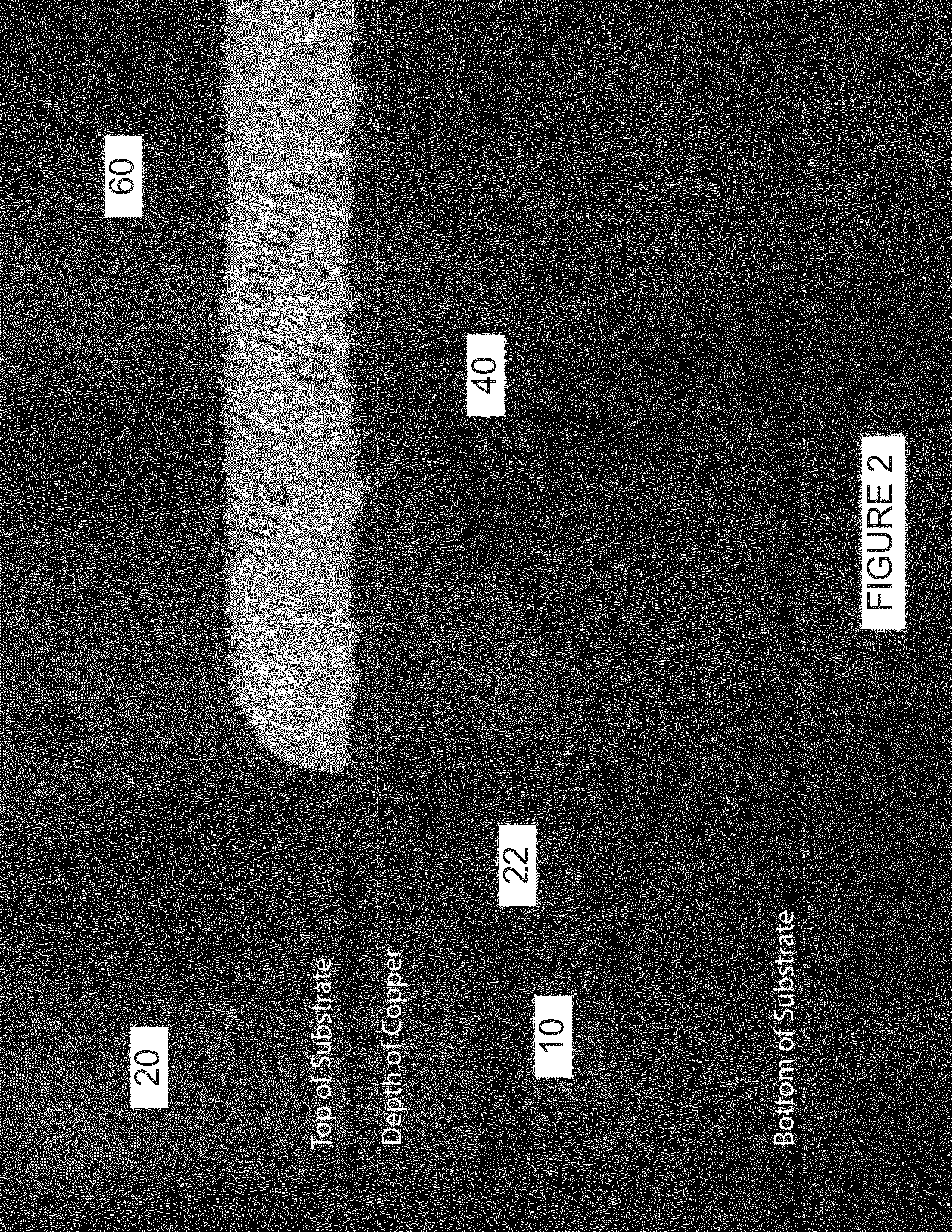
[0073]An exemplary embodiment will now be described for illustration.
[0074]For the purpose of showing detailed information and design, the high speed electroless process will focus upon copper to be deposited at a higher rate than the industry norm, which is 1μ-3μ per hour, depending upon the electroless copper chemistries available on the market, and available. Electroless copper plating has been catalyzed, in the past, by an active palladium surface, and continues to deposit auto-catalytically on the newly reduced copper deposited. The deposition rate depends upon the half-reaction activity of the cupric ion reduction and formaldehyde oxidation on the active palladium and copper surfaces. The complexing agents can change the behavior of the half-reactions by stabilizing the cupric ion through complexation and by surface adsorption. Let's examine the complexing agents, ethylenediaminetetraacetic acid and triethanolamine (for example) on the electrochemical reduction of cupric ions ...
PUM
| Property | Measurement | Unit |
|---|---|---|
| conductive | aaaaa | aaaaa |
| thickness | aaaaa | aaaaa |
| degree of density | aaaaa | aaaaa |
Abstract
Description
Claims
Application Information