PROCESS FOR FABRICATING FIN-TYPE FIELD EFFECT TRANSISTOR (FinFET) STRUCTURE AND PRODUCT THEREOF

a field effect transistor and finfet technology, applied in the field of semiconductor process, can solve problems such as short circui

Active Publication Date: 2015-04-02
UNITED MICROELECTRONICS CORP
View PDF9 Cites 52 Cited by
  • Summary
  • Abstract
  • Description
  • Claims
  • Application Information

AI Technical Summary

Benefits of technology

[0006]In view of the foregoing, this invention provides a process for fabricating a fin- type field effect transistor (FinFET) structure.

Problems solved by technology

However, because the piece of the semiconductor compound grown based on the recessed portions of a fin grows also in the lateral direction, it may contact with a piece of the semiconductor compound on a neighboring fin to cause a short circuit.

Method used


Image

  • PROCESS FOR FABRICATING FIN-TYPE FIELD EFFECT TRANSISTOR (FinFET) STRUCTURE AND PRODUCT THEREOF
  • PROCESS FOR FABRICATING FIN-TYPE FIELD EFFECT TRANSISTOR (FinFET) STRUCTURE AND PRODUCT THEREOF
  • PROCESS FOR FABRICATING FIN-TYPE FIELD EFFECT TRANSISTOR (FinFET) STRUCTURE AND PRODUCT THEREOF

Examples


Embodiment Construction

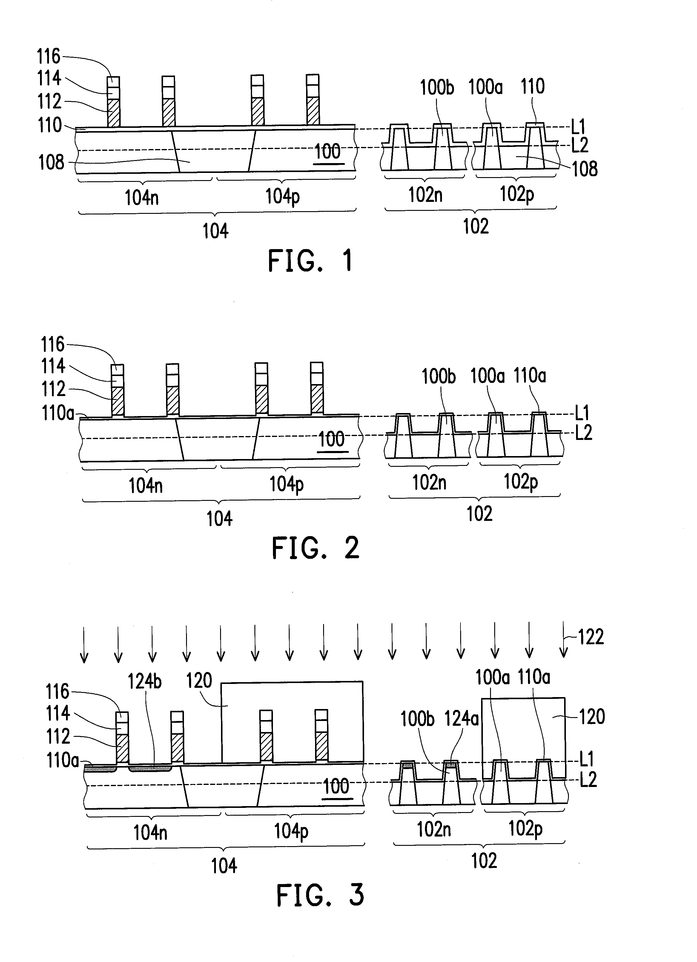
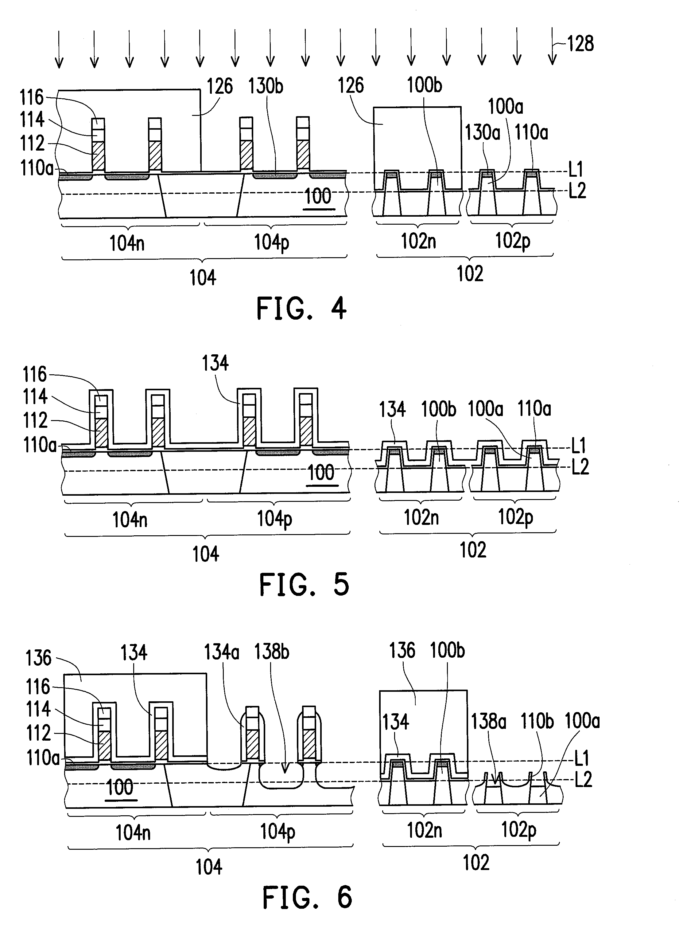
[0018]It is noted that the following embodiment is intended to further explain this invention but not to limit the scope thereof. For example, though the semiconductor compound of the P-type FinFET is formed first in the embodiment, it is also possible to form the semiconductor compound of the N-type FinFET first in other embodiments. In such cases, it is possible that the first semiconductor compound comprises silicon phosphorous (SiP) and the second semiconductor compound comprises SiGe.

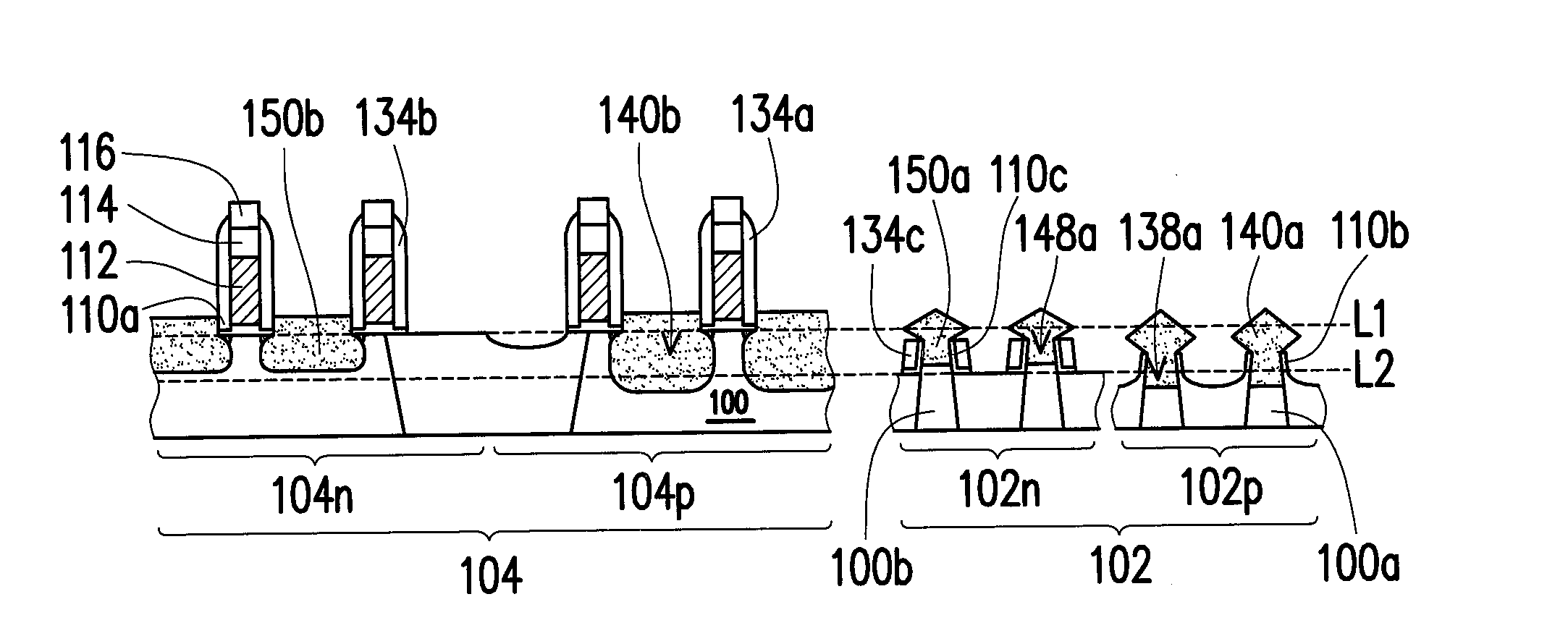
[0019]FIGS. 1-11 illustrate, in a cross-sectional view, a process for fabricating a FinFET structure according to an embodiment of this invention, which is integrated with a fabrication process of ordinary strained CMOS devices.

[0020]Referring to FIG. 1, a semiconductor substrate 100 is provided, which may be a single-crystal silicon substrate. The substrate 100 includes a FinFET area 102 and an ordinary device area 104. The FinFET area 102 includes a NMOS area 102n and a PMOS area 102p. The ordina...


PUM


Abstract

A process for fabricating a fin-type field effect transistor (FinFET) structure is described. A semiconductor substrate is patterned to form a fin. A spacer is formed on the sidewall of the fin. A portion of the fin is removed, such that the spacer and the surface of the remaining fm together define a cavity. A piece of a semiconductor compound is formed from the cavity, wherein the upper portion of the piece of the semiconductor compound laterally extends over the spacer.

Description

BACKGROUND OF THE INVENTION[0001]1. Field of Invention[0002]This invention relates to a semiconductor process and a product thereof, and more particularly relates to a process for fabricating a fin-type field effect transistor (FinFET) structure, and a FinFET structure fabricated through the process.[0003]2. Description of Related Art[0004]A FinFET typically includes a semiconductor fin, a gate crossing over the fin to form a tri-gate structure, and a source and a drain beside the portion of the fin under the gate. In a strained silicon process applied to FinFET, the portions of the fin not under the gate are recessed after the gate is formed, and a semiconductor compound having a lattice parameter different from that of the material of the fin is grown based on the recessed portions of the fin to serve as a source and a drain.[0005]However, because the piece of the semiconductor compound grown based on the recessed portions of a fin grows also in the lateral direction, it may conta...

Claims


Application Information

Patent Timeline
Patent Type & Authority Applications(United States)
IPC IPC(8): H01L29/66H01L29/267H01L29/78
CPCH01L29/66795H01L29/267H01L29/66431H01L29/785H01L21/823807H01L21/823814H01L21/823821H01L29/165H01L29/66636H01L29/7834H01L29/7848
Inventor HUNG, YU-HSIANGFU, SSU-ICHANG, CHUNG-FUWU, YEN-LIANGFAN, CHO-HANLIN, CHIEN-TING
Owner UNITED MICROELECTRONICS CORP
Why Eureka
Try Eureka