Process for etching metal using a combination of plasma and solid state sources

a technology of plasma and solid state sources, applied in the direction of electrical equipment, electrical discharge tubes, conductive material removal by irradiation, etc., can solve the problems of difficult patterning of metals, deleterious effects on semiconductor devices as well as the chamber, and difficult removal of residues

Inactive Publication Date: 2015-04-09
APPLIED MATERIALS INC
View PDF4 Cites 37 Cited by
  • Summary
  • Abstract
  • Description
  • Claims
  • Application Information

AI Technical Summary

Benefits of technology

[0004]Methods of removing etch residue from a substrate as well as from the interior surfaces of an etch process chamber are described. A plasma treatment transforms a metal on the substrate into metal byproducts that deposit on t...

Problems solved by technology

On the other hand, such metals are difficult to pattern.
Such residues can be difficult ...

Method used


Image

  • Process for etching metal using a combination of plasma and solid state sources
  • Process for etching metal using a combination of plasma and solid state sources
  • Process for etching metal using a combination of plasma and solid state sources

Examples


Embodiment Construction

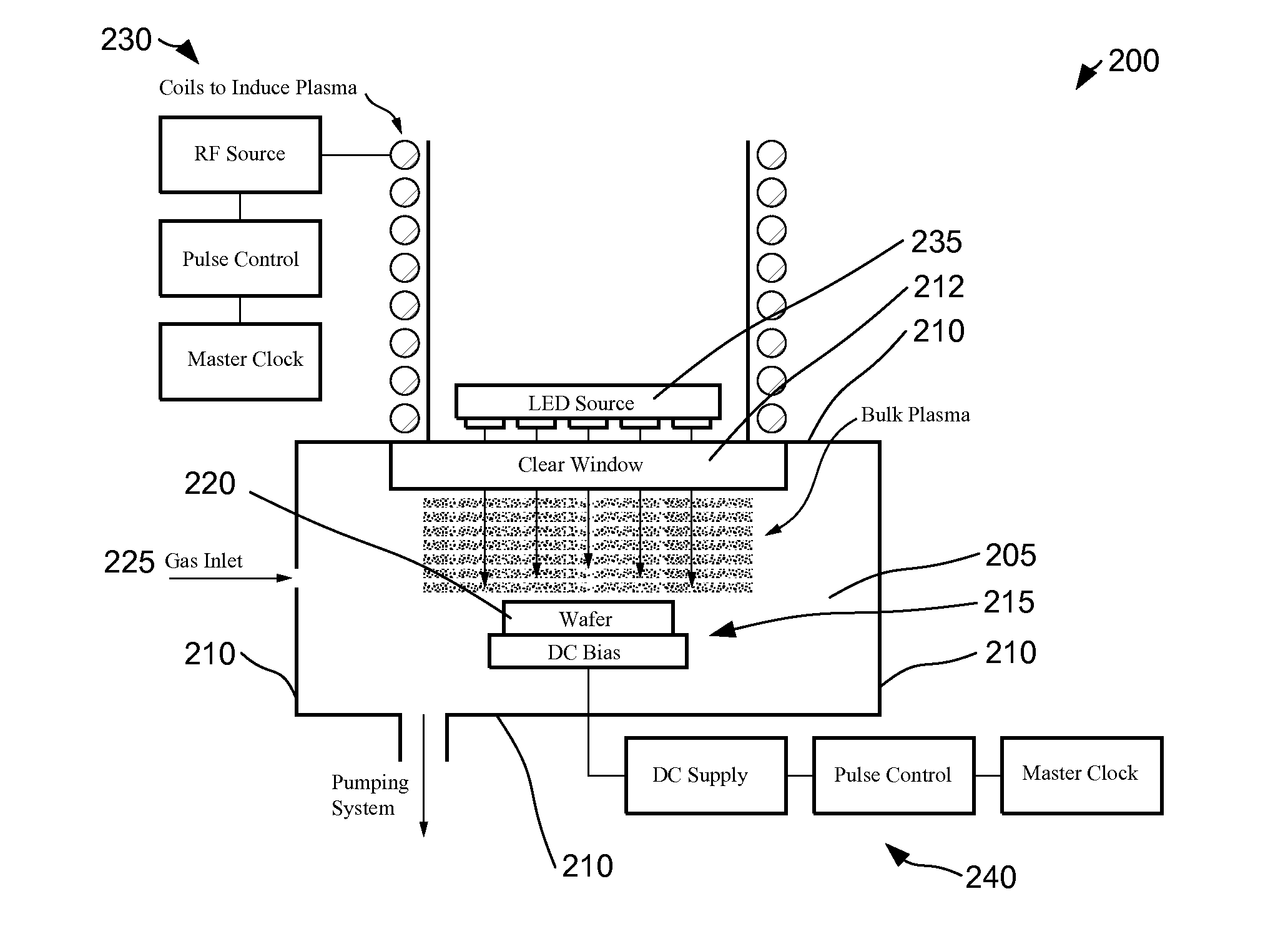
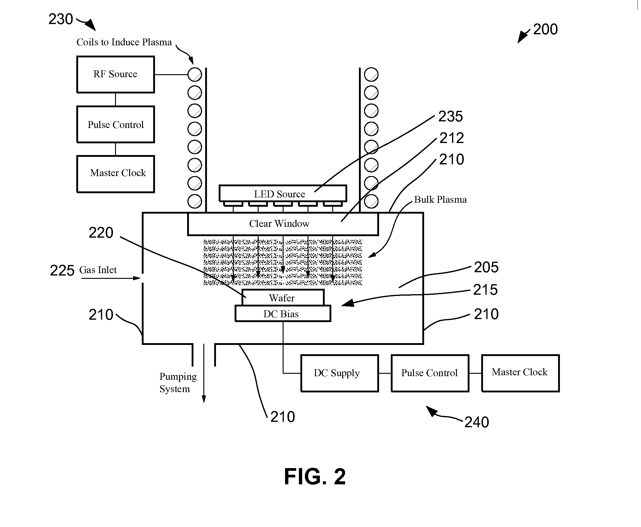
[0012]Certain embodiments of the present invention relate to a method that is useful for the fabrication of semiconductor devices. While the present invention can be useful to produce a wide variety of semiconductor devices, some embodiments of the invention are particularly useful for producing semiconductor devices having metallic layers subtractively patterned with a plasma process, as described in more detail below. It is understood, however, that such a process may also be employed to subtractively pattern non-metallic layers and remove subsequent residues.

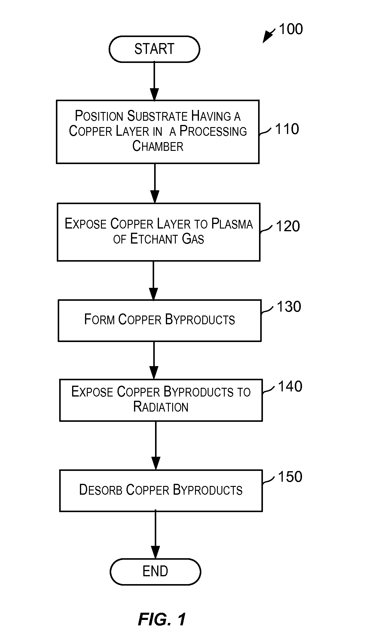
[0013]Methods of removing copper byproducts from the surface of a substrate and from the interior surfaces of an etch process chamber are described. A substrate having a copper layer is placed in the chamber. A plasma treatment transforms the copper into copper containing byproducts that deposit on the substrate and the interior surfaces of the chamber. UV energy is used to desorb the copper containing byproducts so they can ...


PUM

PropertyMeasurementUnit
Angleaaaaaaaaaa
Nanoscale particle sizeaaaaaaaaaa
Wavelengthaaaaaaaaaa

Abstract

An apparatus configured to remove metal etch byproducts from the surface of substrates and from the interior of a substrate processing chamber. A plasma is used in combination with a solid state light source, such as an LED, to desorb metal etch byproducts. The desorbed byproducts may then be removed from the chamber.

Description

CROSS-REFERENCES TO RELATED APPLICATIONS[0001]This application claims priority to Provisional Application No. 61 / 887,830, filed Oct. 7, 2013, titled “APPARATUS FOR ETCHING SUBSTRATES PRODUCING NON-VOLATILE BYPRODUCTS USING COMBINATION OF PLASMA AND LED SOURCES” and Provisional Application No. 61 / 886,521, filed Oct. 3, 2013, titled “LED BASED OPTICAL SOURCE COUPLED WITH PLASMA SOURCE”, which are hereby incorporated by reference in their entirety.BACKGROUND OF THE INVENTION[0002]The use of metals such as copper and cobalt as a conductive interconnect material is favored in semiconductor devices because of the high electrical conductivities and circuit speeds these metals enable. On the other hand, such metals are difficult to pattern. As such, copper interconnect leads have predominantly heretofore been formed using damascene and dual damascene processing technology whereby openings are formed in a dielectric layer on a substrate such as a semiconductor substrate used to form semicond...

Claims


Application Information

Patent Timeline
IPC IPC(8): H01L21/3213H01L21/268
CPCH01L21/32136H01L21/2686H01L21/268H01J37/321H01J2237/3343H01L21/02071H01J37/32862H01J37/32146C23F4/00H01L21/3065H01L21/31116H01L21/32135H05K3/027
Inventor DESHMUKH, SUBHASHJOHNSON, JOSEPHLIU, JINGJINGREN, HE
Owner APPLIED MATERIALS INC
Why Eureka
Try Eureka