Light-Emitting Element, Light-Emitting Device, Electronic Device, and Lighting Device

a technology of light-emitting devices and light-emitting elements, which is applied in the direction of solid-state devices, semiconductor devices, thermoelectric devices, etc., can solve the problems of low utility value and difficult commercialization, and achieve stable state, favorable characteristics after long-time driving, and good

Active Publication Date: 2015-04-16
SEMICON ENERGY LAB CO LTD
View PDF2 Cites 47 Cited by
  • Summary
  • Abstract
  • Description
  • Claims
  • Application Information

AI Technical Summary

Benefits of technology

[0010]One embodiment of the present invention is a light-emitting element including an EL layer between a pair of electrodes. A light-emitting layer included in the EL layer has a stacked-layer structure which is different from the conventional structure, whereby the light-emitting element can keep favorable characteristics after long-time driving even in the case where carrier balance is changed over time due to driving of the light-emitting element or a light-emitting region is shifted due to the change.
[0011]Specifically, in the case where the light-emitting layer included in the EL layer of the light-emitting element has a stacked-layer structure and the stacked light-emitting layers contain different light-emitting materials, a light-emitting layer having the same structure as that of a light-emitting layer that contains a light-emitting material exhibiting emission at a short wavelength is further provided, and a light-emitting layer that contains a light-emitting material exhibiting emission at a long wavelength is sandwiched between the two light-emitting layers each of which contains a light-emitting material exhibiting emission at a short wavelength. As a result, even in the case where the light-emitting region is shifted due to the change in carrier balance in each stacked light-emitting layer or between the light-emitting layers, another light-emitting layer can compensate for the change and the stable state in the whole light-emitting layer can be kept; thus, a light-emitting element that can keep the favorable characteristics after long-time driving can be obtained.

Problems solved by technology

Even if the characteristics of the light-emitting element in the initial stage are favorable, in the case where the light-emitting element cannot withstand long-time driving and the lifetime as an element is short, the utility value is low and the commercialization is difficult.

Method used


Image

  • Light-Emitting Element, Light-Emitting Device, Electronic Device, and Lighting Device
  • Light-Emitting Element, Light-Emitting Device, Electronic Device, and Lighting Device
  • Light-Emitting Element, Light-Emitting Device, Electronic Device, and Lighting Device

Examples


embodiment 1

[0059]In this embodiment, a light-emitting element which is one embodiment of the present invention will be described.

[0060]The light-emitting element of one embodiment of the present invention is formed by providing an EL layer including a light-emitting layer between a pair of electrodes. The light-emitting layer has a stacked-layer structure of: a first light-emitting layer including at least a first light-emitting material (also referred to as a guest material), an electron-transport material (also referred to as a host material), and a hole-transport material (also referred to as an assist material); a second light-emitting layer including at least a second light-emitting material, the electron-transport material, and the hole-transport material; and a third light-emitting layer including at least the first light-emitting material, the electron-transport material, and the hole-transport material.

[0061]An element structure of the light-emitting element of one embodiment of the p...

embodiment 2

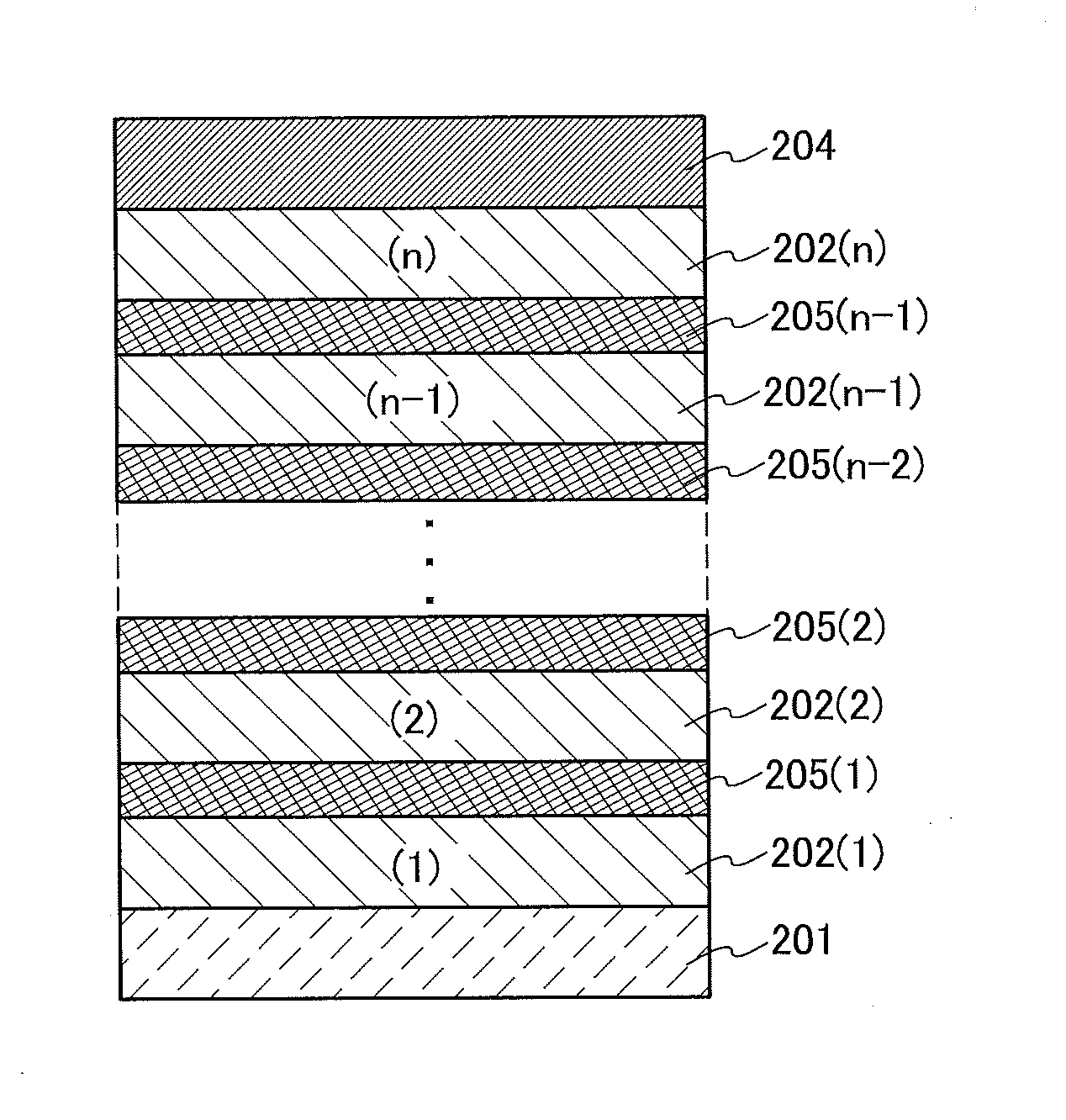
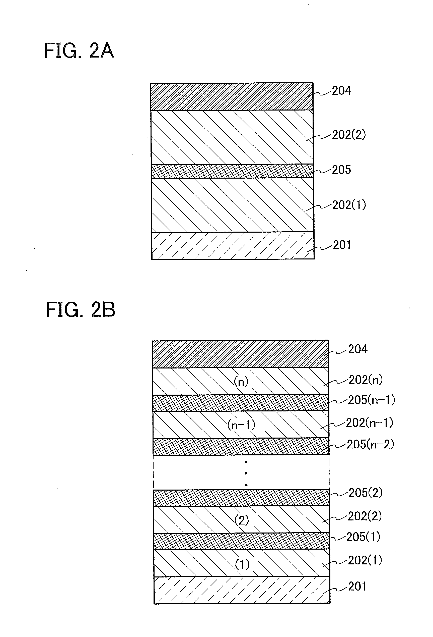
[0093]In this embodiment, as one embodiment of the present invention, a light-emitting element (hereinafter referred to as tandem light-emitting element) in which a charge-generation layer is provided between a plurality of EL layers is described with reference to FIGS. 2A and 2B.

[0094]A light-emitting element described in this embodiment is a tandem light-emitting element including a plurality of EL layers (a first EL layer 202(1) and a second EL layer 202(2)) between a pair of electrodes (a first electrode 201 and a second electrode 204) as illustrated in FIG. 2A.

[0095]In this embodiment, the first electrode 201 functions as an anode, and the second electrode 204 functions as a cathode. Note that the first electrode 201 and the second electrode 204 can have structures similar to those described in Embodiment 1. In addition, all or any of the plurality of EL layers (the first EL layer 202(1) and the second EL layer 202(2)) may have structures similar to those described in Embodimen...

embodiment 3

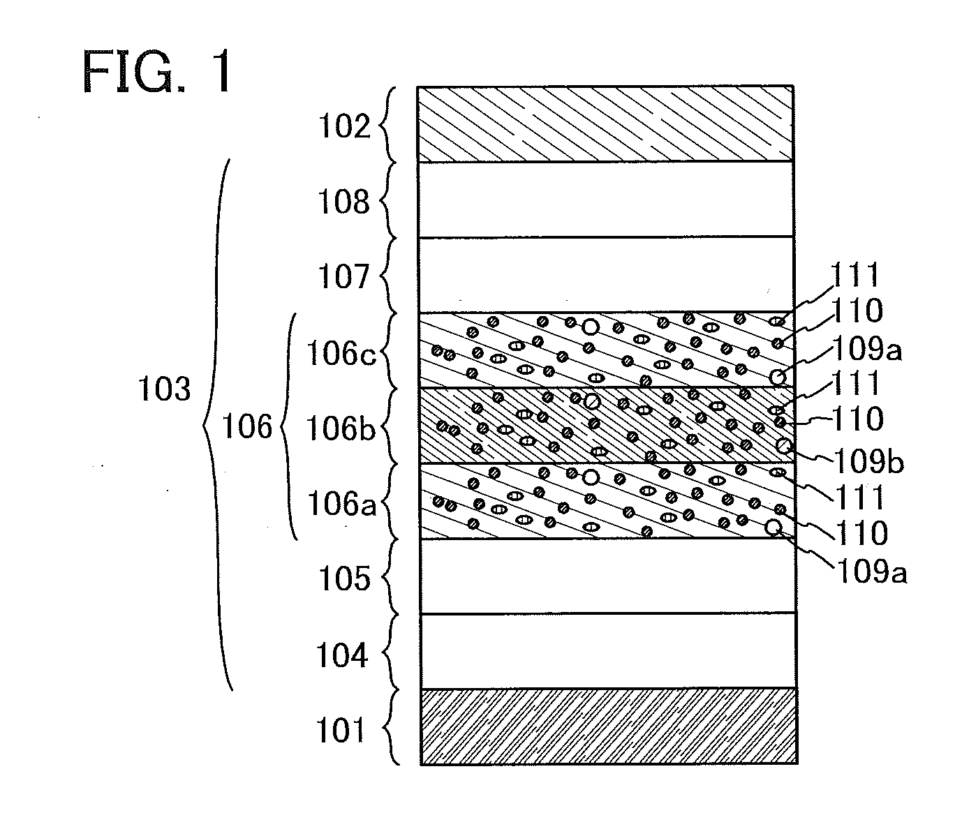
[0110]In this embodiment, a light-emitting device which is one embodiment of the present invention will be described.

[0111]A light-emitting device described in this embodiment has a micro optical resonator (microcavity) structure in which a light resonant effect between a pair of electrodes is utilized. The light-emitting device includes a plurality of light-emitting elements each of which has at least an EL layer 305 between a pair of electrodes (a reflective electrode 301 and a transflective electrode 302) as illustrated in FIG. 3. The EL layer 305 includes at least a light-emitting layer 304 serving as a light-emitting area and may further include a hole-injection layer, a hole-transport layer, an electron-transport layer, an electron-injection layer, a charge-generation layer, and the like.

[0112]In this embodiment, a light-emitting device is described which includes two kinds of light-emitting elements (a first light-emitting element 310R and a second light-emitting element 310G...


PUM


Abstract

A light-emitting element with high reliability that can keep favorable characteristics after long-time driving is provided. In addition, a light-emitting device having a long lifetime including the light-emitting element is provided. Moreover, an electronic device and a lighting device having a long lifetime are provided. In a light-emitting element including an EL layer between a pair of electrodes, a light-emitting layer included in the EL layer has a stacked-layer structure which is different from the conventional structure, whereby the light-emitting element can keep favorable characteristics after long-time driving even in the case where carrier balance is changed over time due to driving of the light-emitting element or a light-emitting region is shifted due to the change.

Description

BACKGROUND OF THE INVENTION[0001]1. Field of the Invention[0002]The present invention relates to an object, a method, or a manufacturing method. In addition, the present invention relates to a process, a machine, manufacture, or a composition of matter. In particular, one embodiment of the present invention relates to a semiconductor device, a display device, a light-emitting device, a lighting device, driving methods thereof, or manufacturing methods thereof. In particular, one embodiment of the present invention relates to a light-emitting element in which an organic compound that emits light by application of an electric field is provided between a pair of electrodes, and also relates to a light-emitting device, an electronic device, and a lighting device including such a light-emitting element.[0003]2. Description of the Related Art[0004]A light-emitting element using an organic compound as a luminous body, which has features such as thinness, lightness, high-speed response, and...

Claims


Application Information

Patent Timeline
Patent Type & Authority Applications(United States)
IPC IPC(8): H01L51/50
CPCH01L51/504H01L51/5056H01L51/5072H10K59/32H10K85/633H10K85/631H10K85/6576H10K85/6572H10K85/342H10K50/13H10K50/11H10K2101/10H10K50/19H10K2101/27H10K2101/90H10K50/125H10K85/615H10K85/636H10K50/15H10K50/16H10K59/12H10K85/622
Inventor SEO, SATOSHIUESAKA, SHOGOYAMAOKA, RYOHEI
Owner SEMICON ENERGY LAB CO LTD
Why Eureka
Try Eureka