
Antistatic structure of array substrate

Active Publication Date: 2015-04-16
TCL CHINA STAR OPTOELECTRONICS TECH CO LTD
View PDF0 Cites 1 Cited by
  • Summary
  • Abstract
  • Description
  • Claims
  • Application Information

AI Technical Summary

Benefits of technology

The present invention provides an antistatic structure for an array substrate that prevents electrostatic damage to metal intersections caused by plasma during a manufacturing process. This results in improved product quality, increased manufacturing efficiency, and lower manufacture costs. The invention includes a dummy wire adjacent to each outermost shorting bar that forms a saw-toothed arrangement. This arrangement helps to protect metal intersections from static electricity damage caused by abnormal discharge.

Problems solved by technology

ESD (Electro-Static Discharge) has long been an unsolved problem of the semiconductor industry.
ESD may lead to reduction of yield rate, increase of cost, and lowering of throughput.
In the manufacture of liquid crystal displays, particularly the manufacture of liquid crystal display panels, ESD has also long affected the quality of the liquid crystal displays.
Any particle may cause damage to a device and even results in discarding.
Further, the raw materials used in these processes may also induce static electricity due to material defects.
The quality of design may directly affect the condition associated with static electricity.
However, in such technology, damages resulting from ESD may still occur at metal intersections of the shorting bars 100 due to abnormal discharge caused by plasma in dry etching operations of the insulation protection layer and the active layer and the quality of a product may thus be affected.

Method used


Image

  • Antistatic structure of array substrate
  • Antistatic structure of array substrate
  • Antistatic structure of array substrate

Examples


Embodiment Construction

[0041]To further expound the technical solution adopted in the present invention and the advantages thereof, a detailed description is given to a preferred embodiment of the present invention and the attached drawings.

[0042]The present invention will be explained with reference to a VA (Vertical Alignment) display mode, but is not limited to the VA display mode.

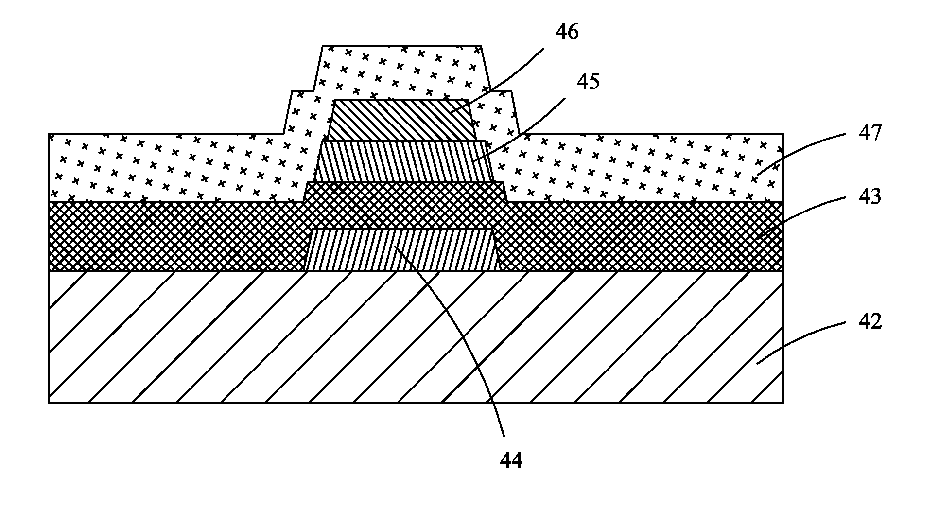
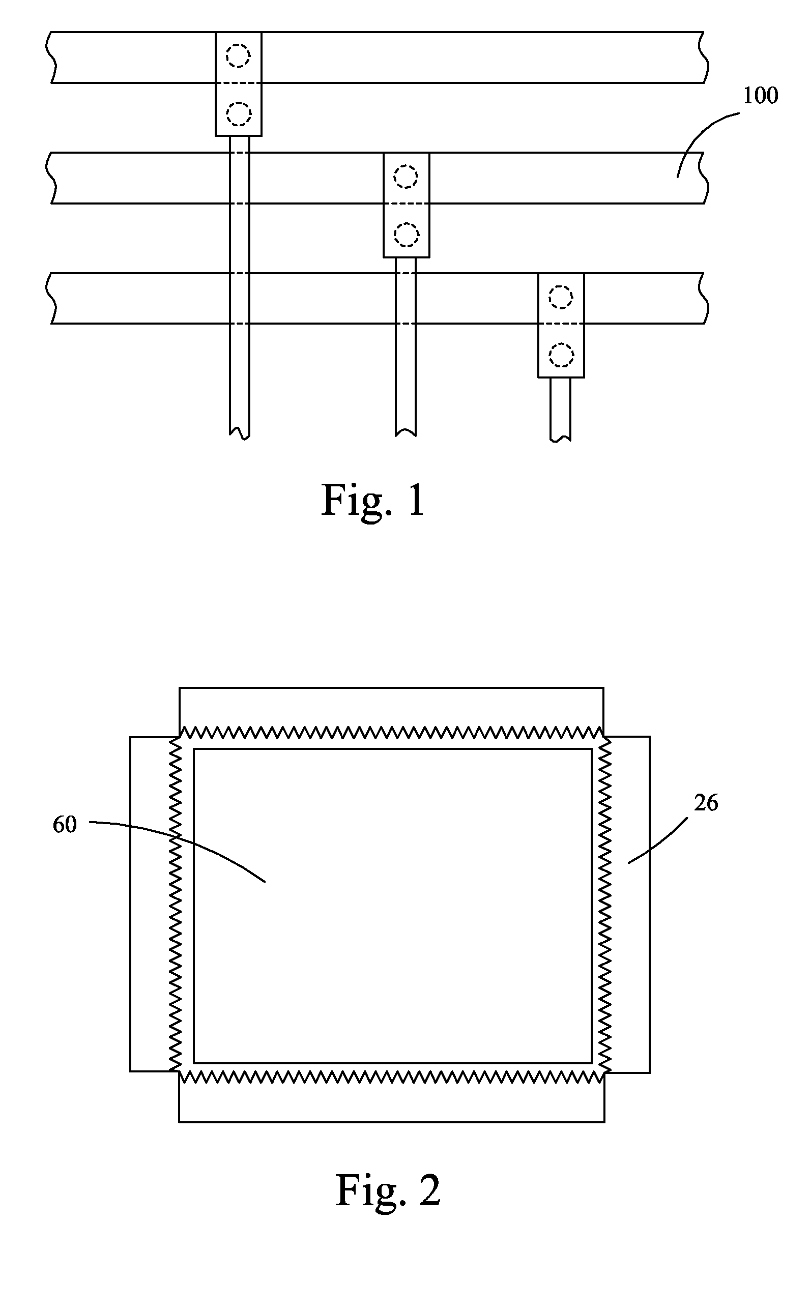
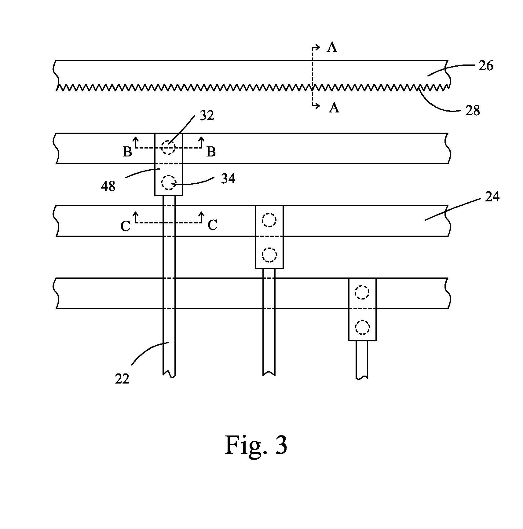
[0043]The present invention provides an arrangement that, in the manufacture of an array substrate, patternizes and forms dummy wires that are parallel to shorting bars at location adjacent to the shorting bars. In other words, the present invention provides an antistatic structure of an array substrate and, as shown in FIGS. 2 and 3, specifically comprises: an effective zone 60 of the array substrate and a plurality of dummy wires 26 surrounding the effective zone 60. The effective zone 60 of the array substrate comprises a plurality of signal wires 22 and a plurality of shorting bars 24 respectively in electrical connection...


PUM


Abstract

The present invention provides an antistatic structure of an array substrate, which includes: an effective zone (60) of an array substrate and a plurality of dummy wires (26) surrounding the effective zone (60). The effective zone (60) includes a plurality of signal wires (22) and a plurality of shorting bars (24) respectively in electrical connection with the plurality of signal wires (22). The dummy wires (26) are set to be respectively corresponding to and adjacent to outermost ones of the shorting bars (24) of the effective zone (60). The dummy wires (26) each include an inner side (28) that is close to the shorting bars (24) and forms a saw-toothed arrangement. The present invention arranges a dummy wire adjacent to each of the outermost ones of shorting bars and the dummy wire has one side that is close to the shorting bar and forms a saw-toothed arrangement. As such, during a manufacturing process of the array substrate, particularly in dry etching operations of an insulation protection layer and an active layer, metal intersections of the shorting bar can be well protected from static electricity damage caused by abnormal discharge resulting from plasma so as to improve product quality.

Description

BACKGROUND OF THE INVENTION[0001]1. Field of the Invention[0002]The present invention relates to the field of displaying technology, and in particular to an antistatic structure of an array substrate.[0003]2. The Related Arts[0004]Liquid crystal displays (LCDs) have a variety of advantages, such as thin device body, low power consumption, and being free of radiation, and are thus widely used. Most of the liquid crystal displays that are currently available in the market are backlighting liquid crystal displays, which comprise a casing, a liquid crystal display panel received in the casing, and a backlight module arranged in the casing to be opposite to the liquid crystal display panel. The operation principle of the liquid crystal display panel is that liquid crystal molecules interposed between two parallel glass substrates and a drive voltage is applied to the two glass substrates to control the rotation of the liquid crystal molecules in order to refract out light emitting from t...

Claims


Application Information

Patent Timeline
IPC IPC(8): G02F1/1362H01L27/12H01L27/02G02F1/1368
CPCG02F1/136204G02F1/1368H01L27/124H01L27/0288
Inventor XU, XIANGYANGCHANG, WEIMINSONG, ZHIYANGWANG, LIANG
Owner TCL CHINA STAR OPTOELECTRONICS TECH CO LTD
Features
  • Generate Ideas
  • Intellectual Property
  • Life Sciences
  • Materials
  • Tech Scout
  • Unparalleled Data Quality
  • Higher Quality Content
  • 60% Fewer Hallucinations
Learn More