Electro-optical device and electronic apparatus

a technology applied in the field of optical devices and electronic devices, can solve problems such as cracks in scanning lines, increased contact holes of dummy pixels, and defects stemming from new causes, and achieve the effect of suppressing the occurrence of defects

Active Publication Date: 2015-04-16
SEIKO EPSON CORP
View PDF7 Cites 27 Cited by
  • Summary
  • Abstract
  • Description
  • Claims
  • Application Information

AI Technical Summary

Benefits of technology

[0007]An advantage of some aspects of the invention is to provide an electro-optical device able to suppress the occurrence of defects stemming from providing a light blocking layer on a dummy pixel, and an electronic apparatus including the electro-optical device.

Problems solved by technology

In a case in which a light blocking layer is provided on the dummy pixel as in the configuration disclosed in JP-A-2005-77636, when a configuration is adopted in which the gate electrode of the transistor is electrically connected to the scanning line via a contact hole formed in the insulating film, a problem arises in that defects stemming from new causes occur.
For example, in a step in which a contact hole that allows the scanning line and gate electrode to be electrically connected, when exposure abnormalities occur in a case of exposure for forming an etching mask, the size of the contact hole of the dummy pixel increases.
Therefore, the insulating film (insulating film between the gate electrode and the light blocking layer in the contact hole) between the contact hole and the light blocking layer becomes thin in the dummy pixel, a stress that occurs at the peripheral edge of the light blocking layer caused by the thermal history in the manufacturing step is added to the scanning line, and cracks occur in the scanning line.
As a result, the scanning line breaks, and the display quality is lowered.

Method used


Image

  • Electro-optical device and electronic apparatus
  • Electro-optical device and electronic apparatus
  • Electro-optical device and electronic apparatus

Examples


Embodiment Construction

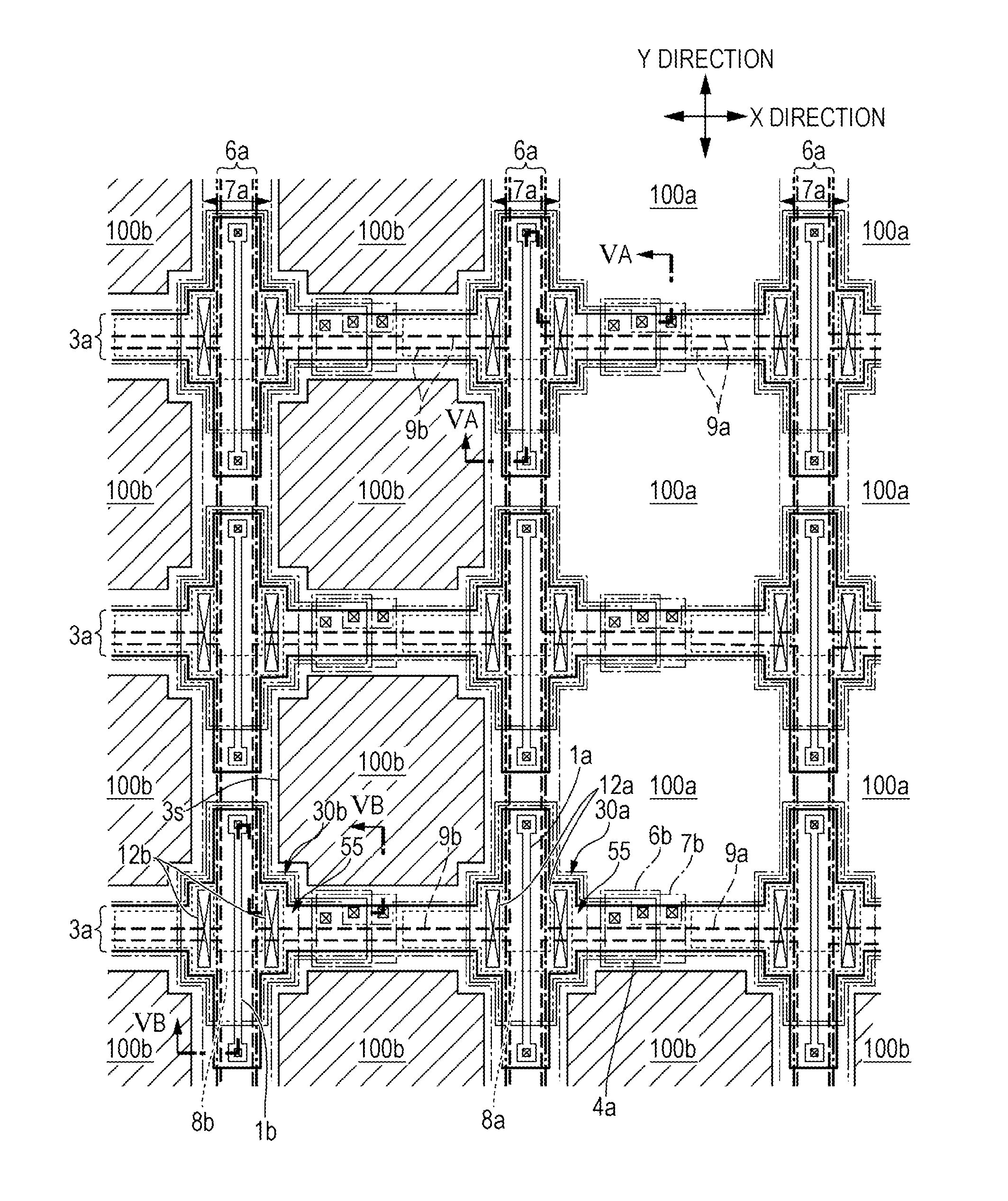
[0029]The electro-optical device according to an embodiment of the invention will be described with reference to the drawings. In the drawings referenced in the following description, the scale is changed for each layer and each member in order to make each layer and each member a visually recognizable size in the drawings. In the drawings referenced in the following description, the numbers of the pixel electrodes, scanning lines, data lines, and the like, are reduced for display. Description is provided in which, from the first direction and second direction that intersect each other in the in-plane direction of the liquid crystal panel, the first direction is the X direction and the second direction is the Y direction.

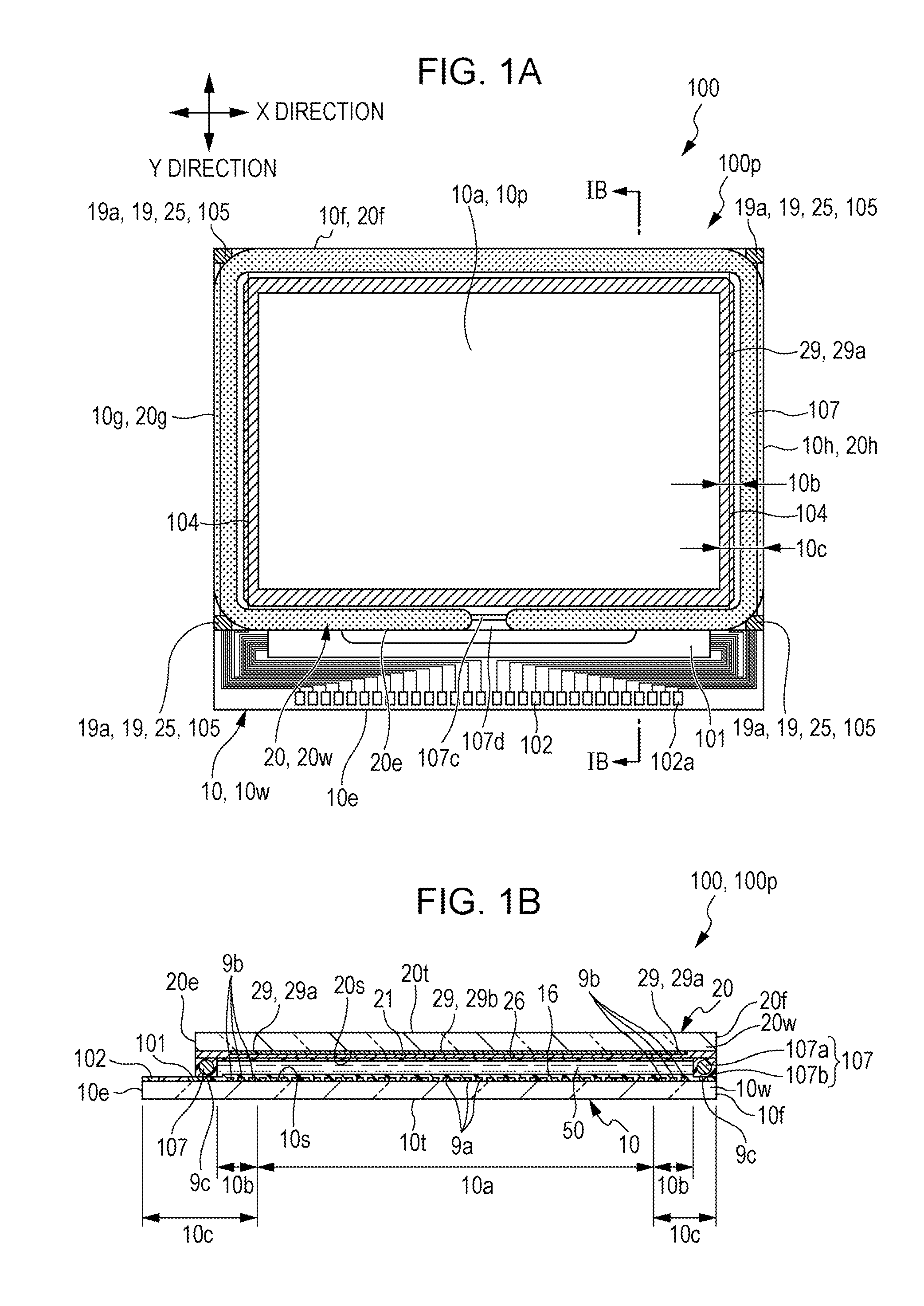
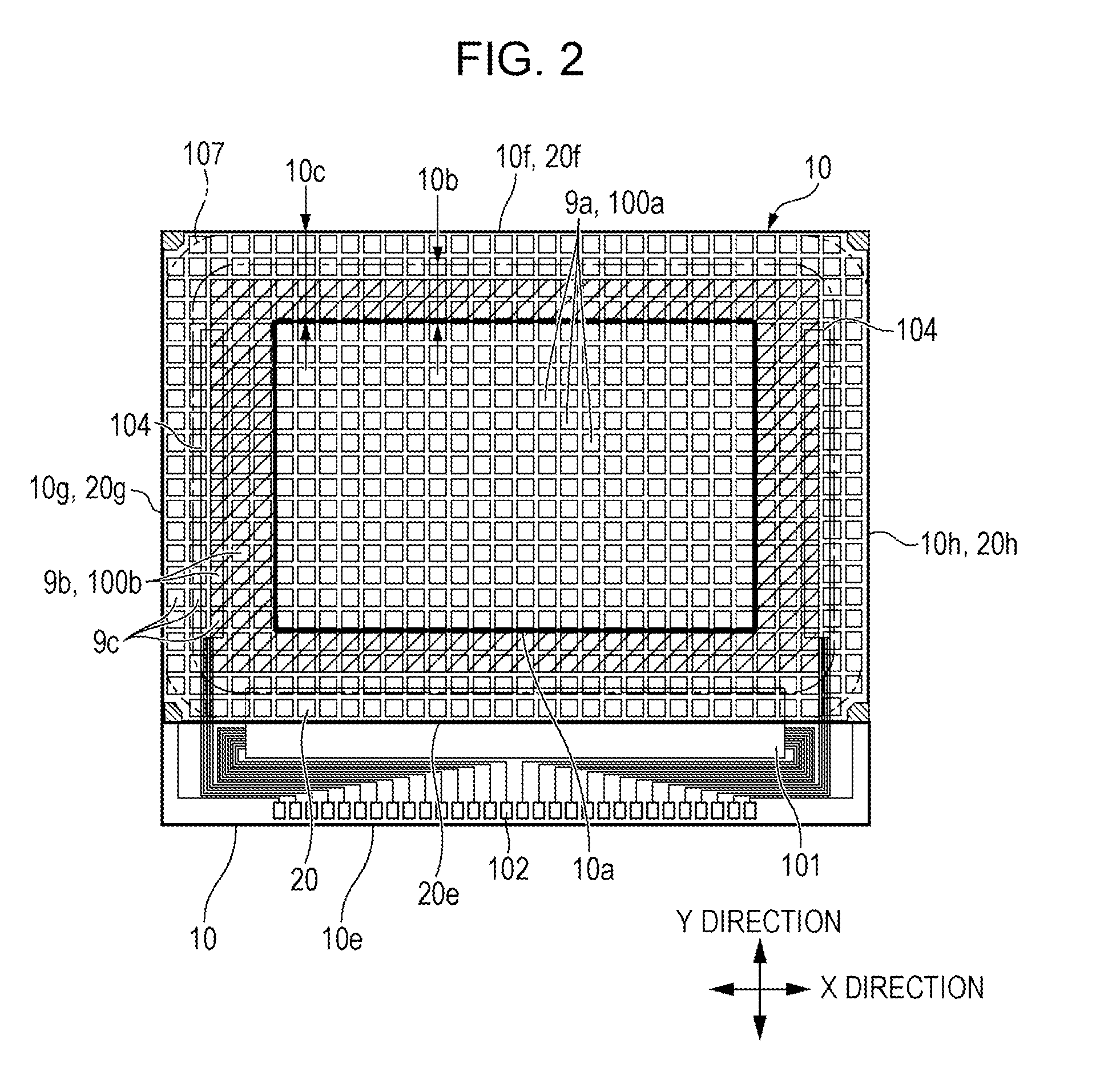
[0030]FIGS. 1A and 1B are explanatory diagrams a liquid crystal panel of the electro-optical device according to the embodiment of the invention. FIGS. 1A and 1B are a planar diagram in which the liquid crystal panel is viewed from the counter substrate side and a c...


PUM

PropertyMeasurementUnit
temperatureaaaaaaaaaa
areaaaaaaaaaaa
dimensionaaaaaaaaaa

Abstract

In a display pixel of an element substrate of an electro-optical device, a first gate electrode of a first transistor is electrically connected to a scanning line via a first contact hole of an insulating film. In a dummy pixel, a light blocking layer of the same layer as the scanning line is formed, and a second gate electrode of a second transistor is electrically connected to a scanning line via a second contact hole. A gap between the end portion of the second contact hole and the end portion of the scanning line is wider than the gap between the end portion of the first contact hole and the end portion of the scanning line.

Description

BACKGROUND[0001]1. Technical Field[0002]The present invention relates to an electro-optical device in which a light blocking layer that overlaps a pixel electrode is provided on a dummy pixel, and an electronic apparatus including the electro-optical device.[0003]2. Related Art[0004]In an electro-optical device, such as a liquid crystal device, a display pixel provided in a display region includes a transistor electrically connected to a scanning line and a pixel electrode electrically connected to the transistor. For the purpose of increasing the quality of the display at the end portions of the display region, a dummy pixel including a transistor electrically connected to the scanning line and a pixel electrode electrically connected to the transistor is provided at the peripheral region that is adjacent at the outer side to the display region, and, for example, a black solid image is displayed in the dummy pixel. However, in a case in which a dummy pixel is provided, since there ...

Claims


Application Information

Patent Timeline
Patent Type & Authority Applications(United States)
IPC IPC(8): G02F1/1362G02F1/1368
CPCG02F1/13624G02F1/1368G02F1/136209G02F1/134336G02F1/133388G02F1/136227H01L27/124
Inventor NAGASAWA, HITOYA
Owner SEIKO EPSON CORP
Why Eureka
Try Eureka