Electrode structure and light emitting diode structure having the same

a technology of light-emitting diodes and electrode structures, which is applied in the direction of basic electric elements, electrical apparatus, and semiconductor devices, can solve the problems of poor reliability analysis severe limits to the life span of the light-emitting diodes, and poor integrity of the conventional barrier layer between the conductive pad and the reflection layer, so as to improve the light-emitting diodes. the effect of reliability analysis and improved light-emi

Active Publication Date: 2015-04-30
LEXTAR ELECTRONICS CORP
View PDF15 Cites 3 Cited by
  • Summary
  • Abstract
  • Description
  • Claims
  • Application Information

AI Technical Summary

Benefits of technology

[0019]In the aforementioned embodiments of the present invention, since the barrier layer having the first and second barrier layers can effectively prevent the chemical combination between the conductive pad and the reflection layer, such that the impedance of the conductive pad is not easily increased for a period of usage time. As a result, the stability of the reliability analysis of the light emitting diode structure may be improved, such that the maximum allowable value of the c

Problems solved by technology

However, after the aluminum reflection layer has been used for a period of time, aluminum corrosion may occur from the conductive pad, which severely limits the life span of the light emitting diode structure.
However, the integrity of the conventional barrier layer between the conductive pad and the reflection layer is poor.
As a result, when the operation voltage is increa

Method used


Image

  • Electrode structure and light emitting diode structure having the same
  • Electrode structure and light emitting diode structure having the same
  • Electrode structure and light emitting diode structure having the same

Examples


Embodiment Construction

[0027]Reference will now be made in detail to the present embodiments of the invention, examples of which are illustrated in the accompanying drawings. Wherever possible, the same reference numbers are used in the drawings and the description to refer to the same or like parts.

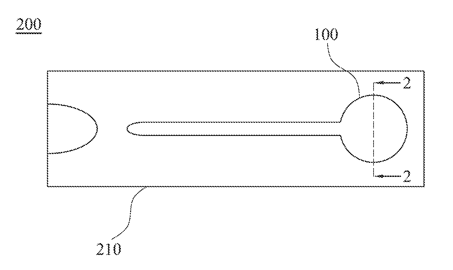
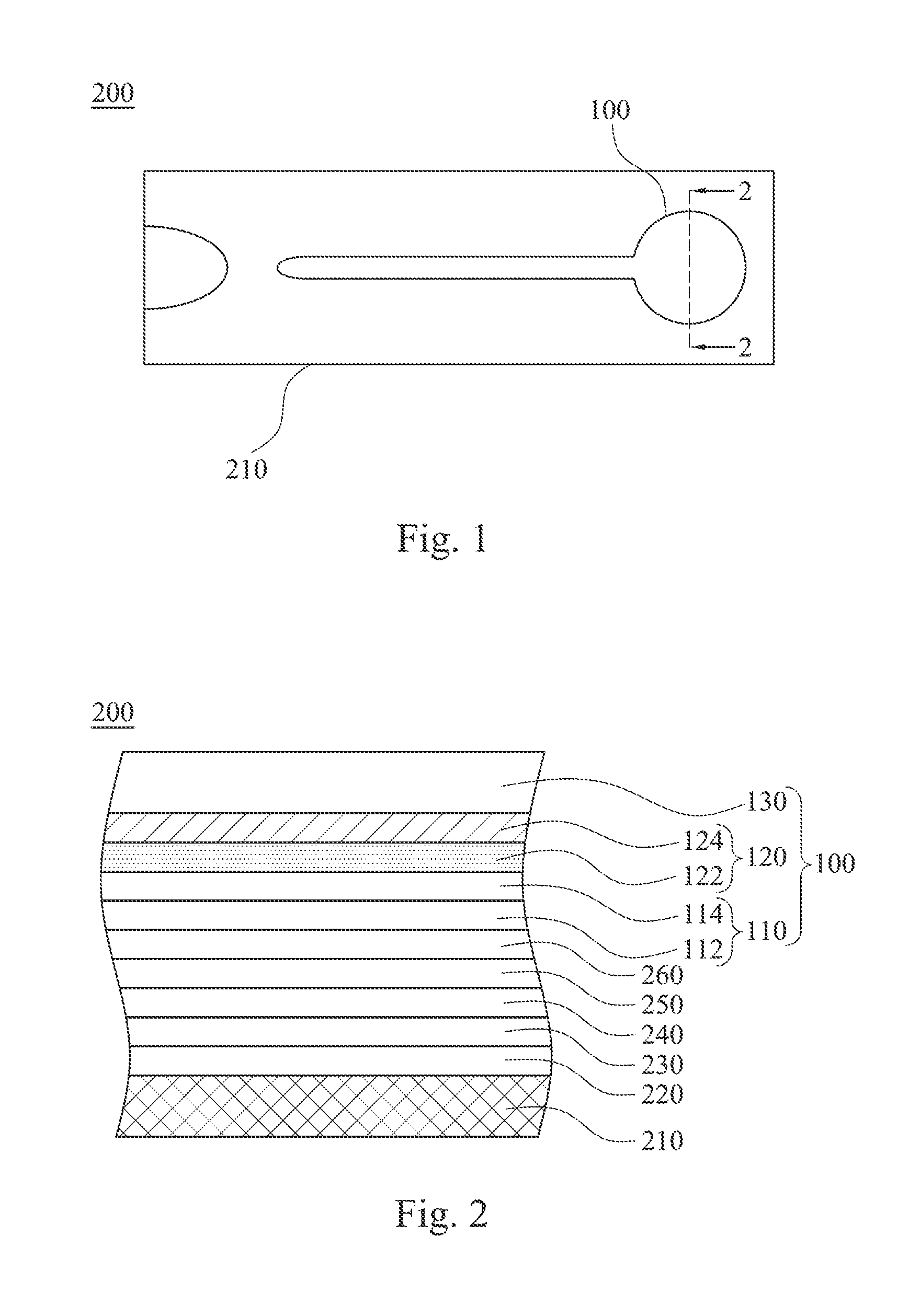
[0028]FIG. 1 is a top view of a light emitting diode structure 200 according to an embodiment of the present invention. FIG. 2 is a cross-sectional view taken along line 2-2 of the light emitting diode structure 200 shown in FIG. 1. As shown in FIG. 1 and FIG. 2, the light emitting diode structure 200 includes a substrate 210, an N-type semiconductor layer 220, a light emitting layer 230, a P-type semiconductor layer 240, and an electrode structure 100. The N-type semiconductor layer 220 is located on the substrate 210. The light emitting layer 230 is located on the N-type semiconductor layer 220. The P-type semiconductor layer 240 is located on the light emitting layer 230. The N-type semiconductor layer 220,...


PUM


Abstract

An electrode structure includes at least one reflection layer, a barrier layer, and a conductive pad. The barrier layer includes a first barrier layer and a second barrier layer. The first and second barrier layers are stacked on the reflection layer in sequence. The first and second barrier layers are made of different materials. The conductive pad is located on the barrier layer.

Description

RELATED APPLICATIONS[0001]This application claims priority to Taiwan Application Serial Number 102138493, filed Oct. 24, 2013, which is herein incorporated by reference.BACKGROUND[0002]1. Field of Invention[0003]The present invention relates to an electrode structure and a light emitting diode structure having the electrode structure.[0004]2. Description of Related Art[0005]A conventional light emitting diode structure is composed of a sapphire substrate, an epitaxial layer (e.g., N-GaN, light emitting layer, and P-GaN), a reflection layer, a barrier layer, and a conductive pad. The epitaxial layer, the reflection layer, the barrier layer, and the conductive pad are formed on the sapphire substrate. The reflection layer is usually made of aluminum to reflect light under the conductive pad, so as to enhance the light emitting efficiency of the light emitting diode structure. However, after the aluminum reflection layer has been used for a period of time, aluminum corrosion may occur ...

Claims


Application Information

Patent Timeline
IPC IPC(8): H01L33/40H01L33/42
CPCH01L33/405H01L33/36H01L33/46H01L33/42
Inventor YANG, TSUNG-YUTSAI, TZONG-LIANG
Owner LEXTAR ELECTRONICS CORP
Why Eureka
Try Eureka