Detection device

a detection device and detection technology, applied in the direction of material analysis, weighing by absorbing components, instruments, etc., can solve the problems of inability to quantitatively evaluate, proposed methods fail to work, and quantitative analysis has not yet been achieved, so as to improve sensitivity, reduce the number of hybrid chip members, and facilitate handling

Inactive Publication Date: 2012-10-18
SEIKO EPSON CORP
View PDF5 Cites 13 Cited by
  • Summary
  • Abstract
  • Description
  • Claims
  • Application Information

AI Technical Summary

Benefits of technology

[0012]In one aspect of the invention, the optical device and the microbalance sensor chip can be disposed side by side in the flow channel in a plan view, or stacked in the flow channel. The hybrid chip having the optical device and the microbalance sensor chip stacked can be provided with the metal nanostructure of the optical device formed on the oscillation electrode of the microbalance sensor chip. According to this configuration, the number of members of the hybrid chip is reduced, and handling becomes easier be

Problems solved by technology

Although surface enhanced Raman scattering can be used for qualitative detection in an infinitesimal concentration of gas molecules due to the electric field enhancement effect of the localized surface plasmon resonance, quantitative analysis has not yet been achieved.
However, when the coverage is low, an individual molecule provides the intensity expressed by Formula 1, and therefore, the quantitative evaluation is difficult.
Therefore, the proposed method fails to work when the adsorption coverage of the detection target molecules is low (e.g., with

Method used


Image

  • Detection device
  • Detection device
  • Detection device

Examples


Embodiment Construction

[0031]Hereinafter, a preferred embodiment of the invention will be described in detail. It should be noted that the embodiment explained below does not limit the content of the invention as set forth in the appended claims, and all of the constituents set forth in the present embodiment are not necessarily essential to the invention.

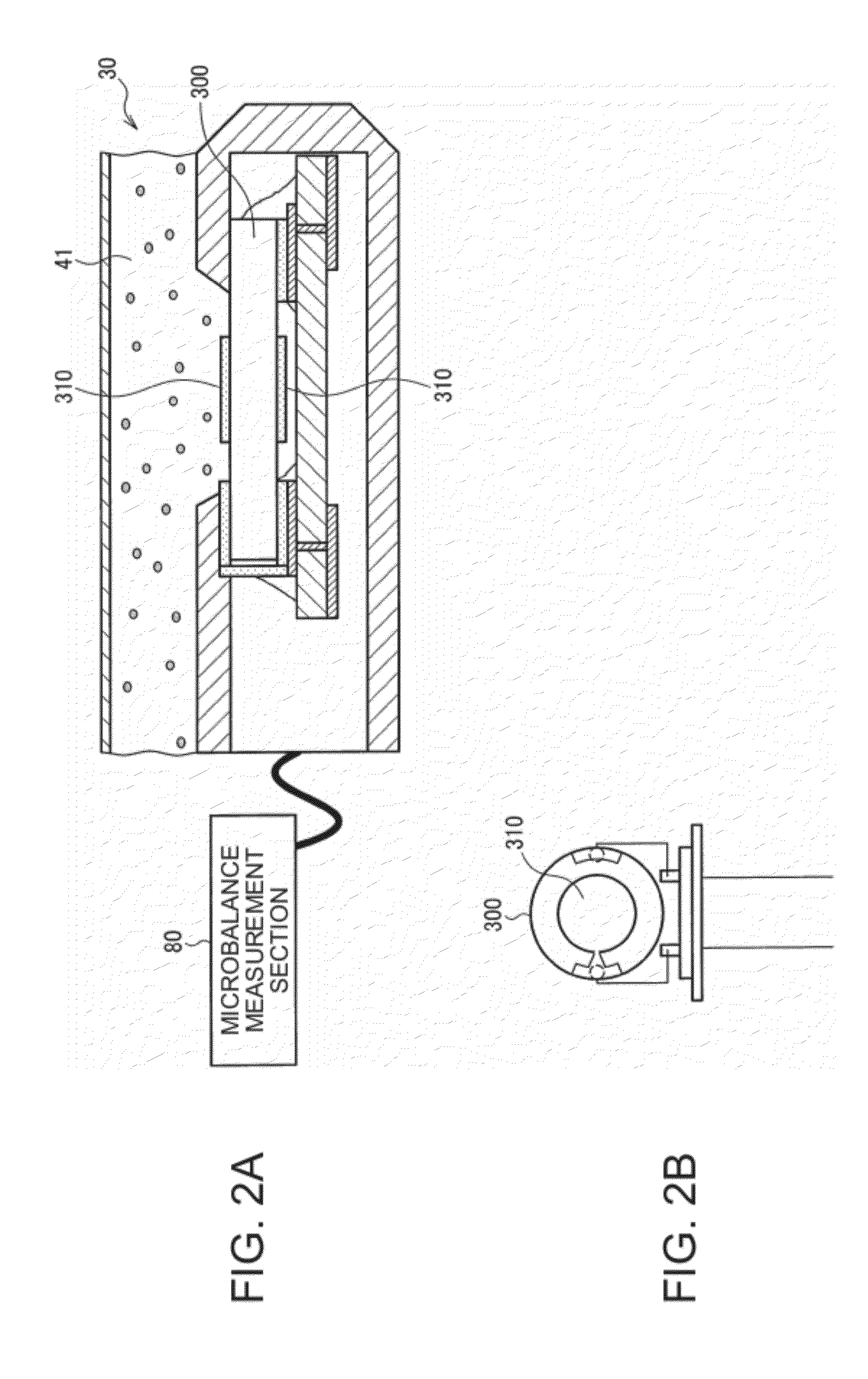
[0032]As shown in FIG. 5 or FIG. 6, the detection device 10A according to the embodiment of the invention is provided with two sensor chips, one is a SERS sensor chip 20 (an optical device), and the other is a microbalance sensor chip 30. These two sensor chips will be explained first.

1. SERS Sensor Chip (Optical Device)

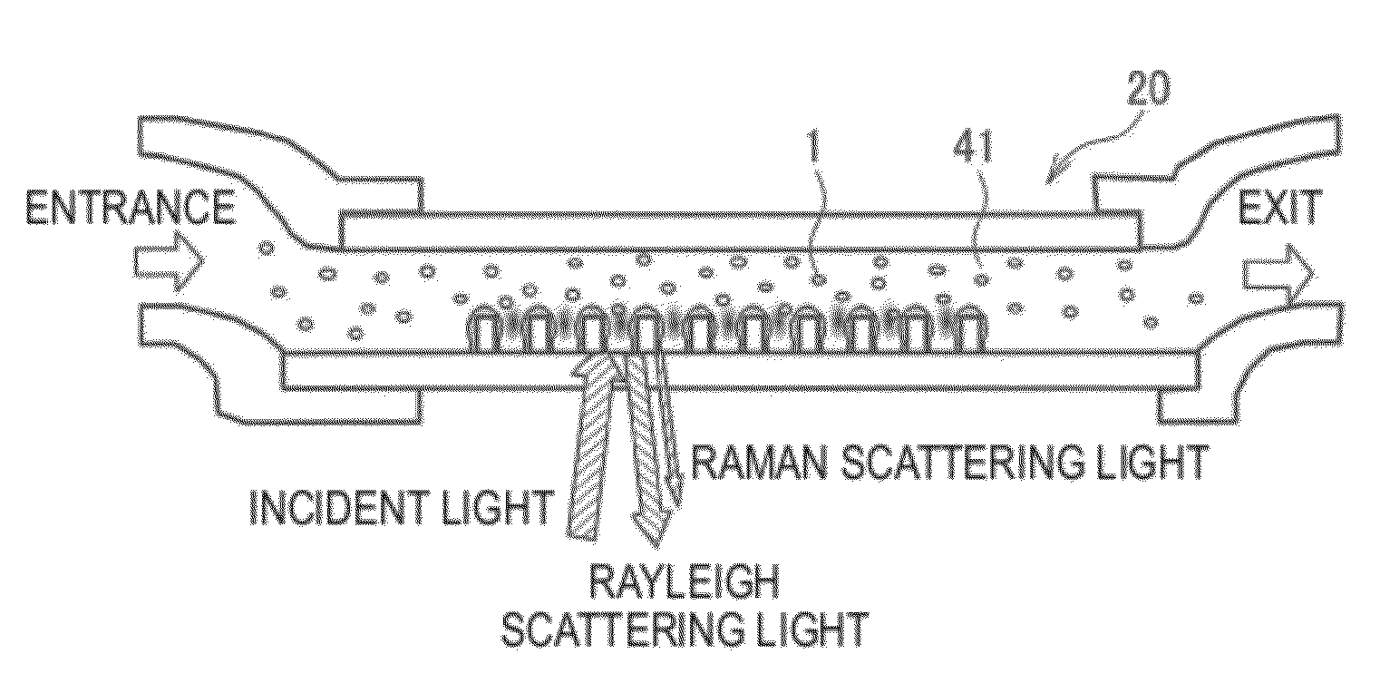
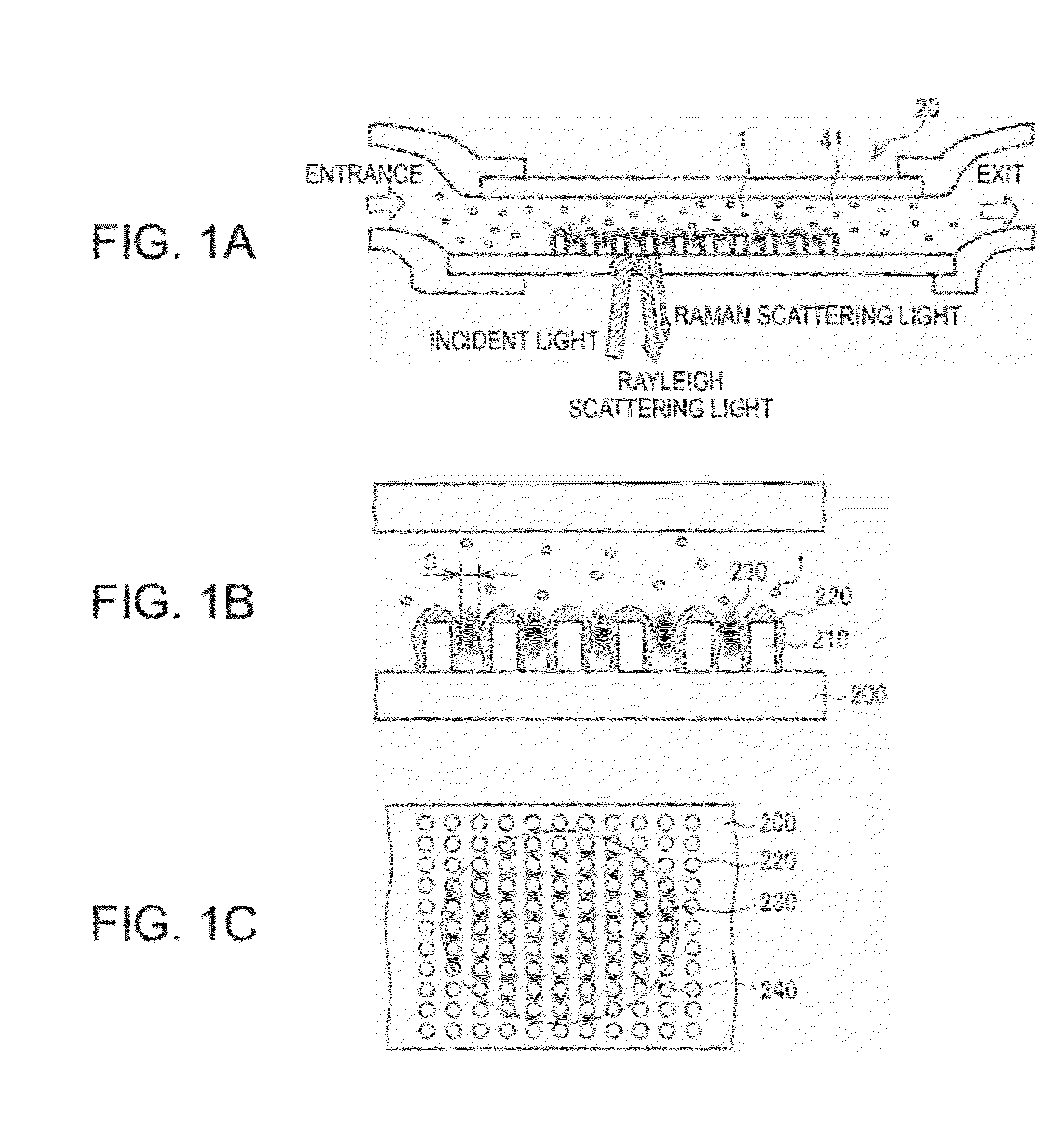
[0033]The sensor chip 20 for detecting the Raman scattering light (an optical device for emitting light corresponding to a fluid sample adsorbed thereto in response to irradiation with light) will be explained with reference to FIGS. 1A through 1C. Explanatory diagrams of the principle will also be shown. It should be noted that in the pr...


PUM


Abstract

A detection device includes a flow channel for a fluid sample, a suction section adapted to draw the fluid sample into the flow channel, an optical device disposed in the flow channel, a light source adapted to irradiate the optical device with light, a light detection section adapted to detect light emitted from the optical device, a microbalance sensor chip having a piezoelectric substrate provided with an oscillation electrode, and disposed in the flow channel, and a quantitative analysis section adapted to perform quantitative analysis on the fluid sample based on output from the light detection section and the microbalance sensor chip. The optical device has a metal nanostructure including projections ranging in size from 1 through 1000 nm, and emits light representing the fluid sample adsorbed to the metal nanostructure.

Description

BACKGROUND[0001]1. Technical Field[0002]The present invention relates to a detection device for performing quantitative analysis on an infinitesimal substance on which qualitative analysis is to be performed.[0003]2. Related Art[0004]In recent years, surface enhanced Raman scattering (SERS) spectroscopy using surface plasmon resonance (SPR), and in particular, localized surface plasmon resonance (LSPR), has been attracting attention as a sensitive spectroscopic technique for detecting low-density sample molecules (e.g., see Japanese Patent No. 3714671, JP-A-2000-356587). Surface enhanced Raman scattering denotes a phenomenon that the Raman scattering light is enhanced 102 through 1014 times on a metal surface having nanometric uneveness. In surface enhanced Raman scattering, the sample molecules are irradiated with an excitation light having a single wavelength such as a laser. The light with a scattering wavelength (the Raman scattering light) shifted from the wavelength of the exc...

Claims


Application Information

Patent Timeline
IPC IPC(8): G01N21/59
CPCG01N29/022G01N5/02G01N21/658G01N2291/0215G01N21/554G01N21/474G01N21/55G01N21/553G01N2291/02809
Inventor YAMADA, KOHEIHASHIMOTO, NOBUAKI
Owner SEIKO EPSON CORP
Why Eureka
Try Eureka