Methods and apparatus for forming flowable dielectric films having low porosity

a flowable dielectric film, low porosity technology, applied in the direction of liquid surface applicators, coatings, chemical vapor deposition coatings, etc., can solve the problems of void-free filling of narrow width, increasing difficulty in void-free filling of high aspect ratio (ar) features, and reducing budgets

Inactive Publication Date: 2015-04-30
LAM RES CORP
View PDF5 Cites 262 Cited by
  • Summary
  • Abstract
  • Description
  • Claims
  • Application Information

AI Technical Summary

Benefits of technology

[0007]Another aspect of the subject matter disclosed herein may be implemented in an apparatus. The apparatus may include a chamber including a substrate support; a plasma generator configured to produce plasma species; one or more inlets to the chamber; and a controller including instructions for: a first operation of introducing a dielectric precursor and a co-reactant to the chamber via the one or more inlets at substrate support temperature of between about −20° C. and 100° C. to thereby form a flowable film; shutting off a flow of the dielectric precursor; and introducing a process gas to the plasma generator no more than 30 seconds after shutting off the dielectric precursor.

Problems solved by technology

As device geometries shrink and thermal budgets are reduced, void-free filling of narrow width, high aspect ratio (AR) features (e.g., AR>6:1) becomes increasingly difficult due to limitations of existing deposition processes.

Method used


Image

  • Methods and apparatus for forming  flowable dielectric films having low porosity
  • Methods and apparatus for forming  flowable dielectric films having low porosity
  • Methods and apparatus for forming  flowable dielectric films having low porosity

Examples


Embodiment Construction

Introduction

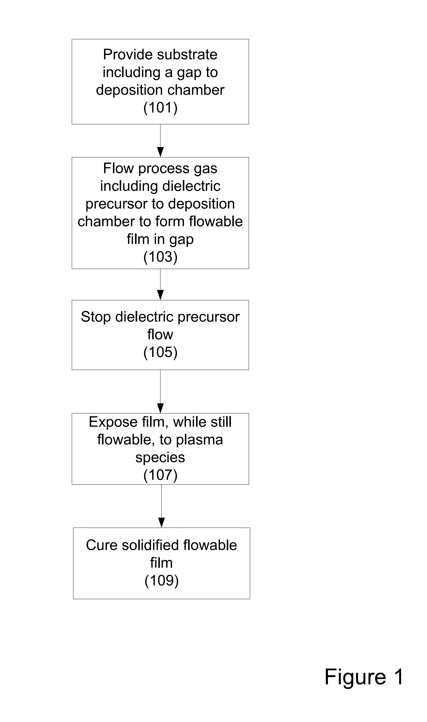
[0016]Aspects of the present invention relate to forming flowable dielectric films on substrates. Some embodiments include filling high aspect ratio gaps with insulating material. For ease of discussion, the description below refers chiefly to flowable silicon oxide films, however the processes described herein may also be used with other types of flowable dielectric films. For example, the dielectric film may be primarily silicon nitride, with Si—N and N—H bonds, primarily silicon oxynitride, primarily silicon carbide or primarily silicon oxycarbide films.

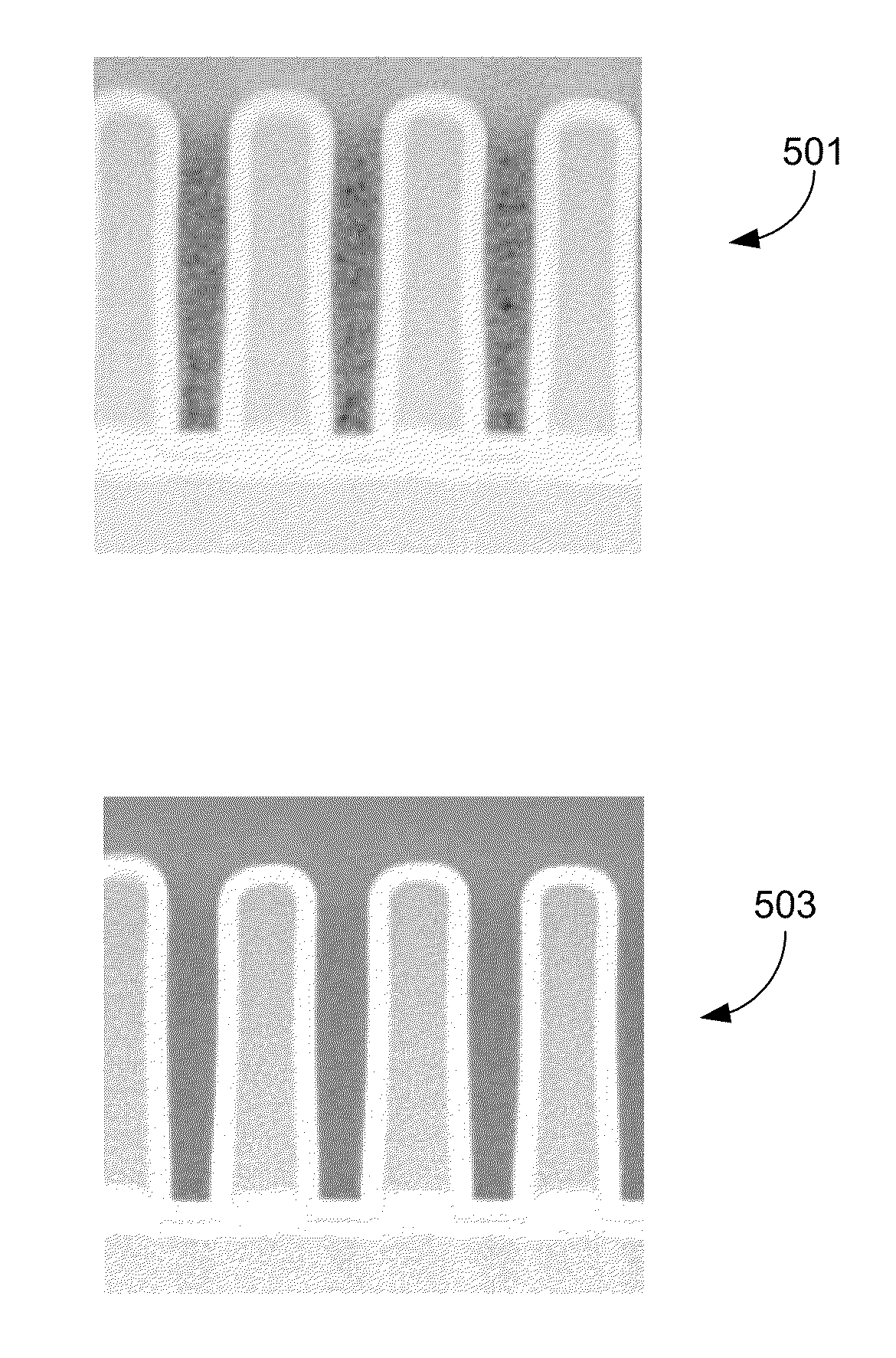
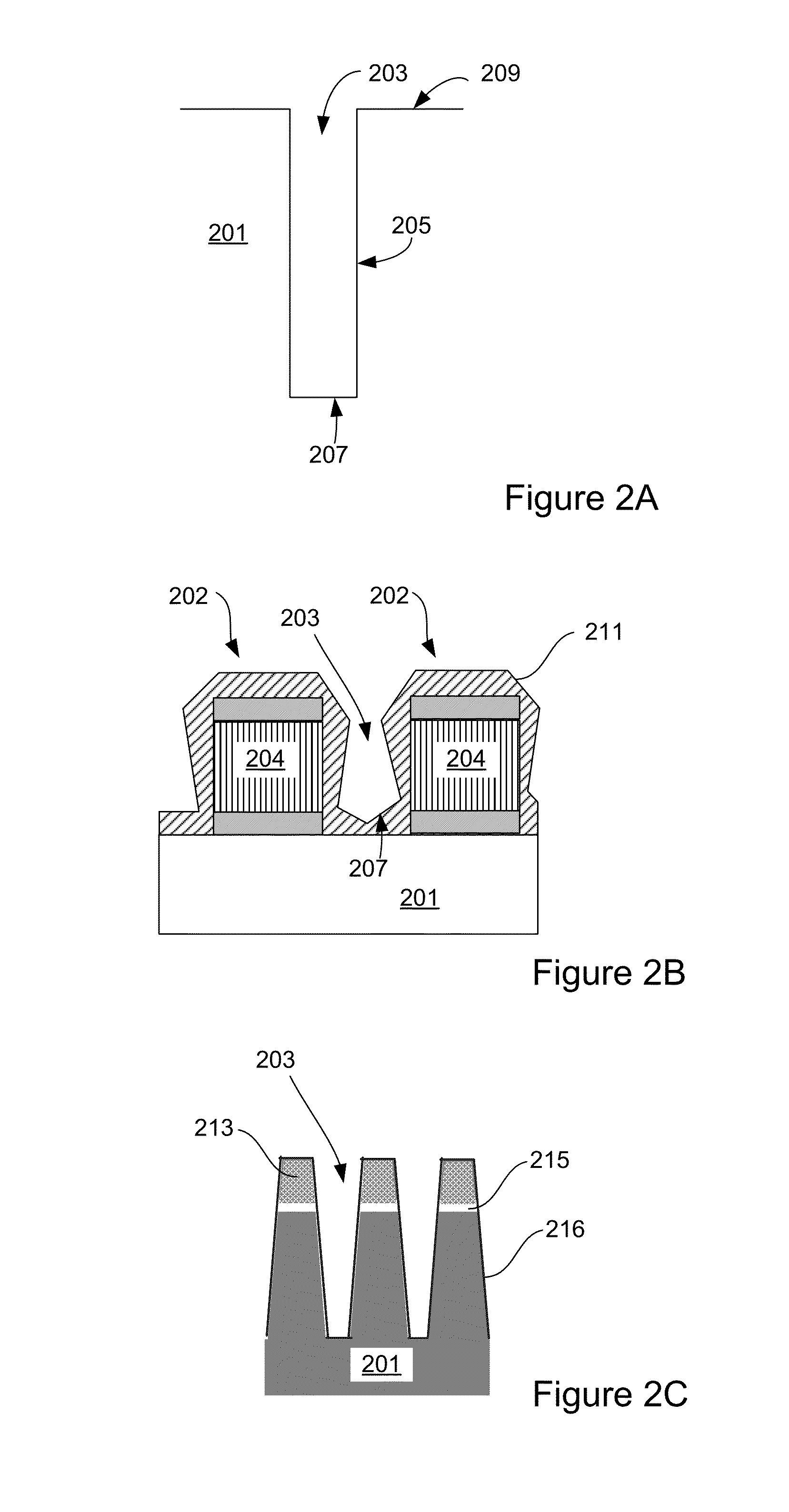
[0017]It is often necessary in semiconductor processing to fill high aspect ratio gaps with insulating material. This is the case for shallow trench isolation (STI), inter-metal dielectric (IMD) layers, inter-layer dielectric (ILD) layers, pre-metal dielectric (PMD) layers, passivation layers, etc. As device geometries shrink and thermal budgets are reduced, void-free filling of narrow width, high aspect ratio (AR) fea...


PUM

PropertyMeasurementUnit
temperatureaaaaaaaaaa
temperaturesaaaaaaaaaa

Abstract

Provided herein are methods and apparatus for forming flowable dielectric films having low porosity. In some embodiments, the methods involve plasma post-treatments of flowable dielectric films. The treatments can involve exposing a flowable film to a plasma while the film is still in a flowable, reactive state but after deposition of new material has ceased.

Description

CROSS-REFERENCE TO RELATED APPLICATION[0001]This application claims priority to U.S. Provisional Patent Application No. 61 / 895,883, filed Oct. 25, 2013, which is incorporated by reference herein in its entirety and for all purposes.BACKGROUND OF THE INVENTION[0002]It is often necessary in semiconductor processing to fill high aspect ratio gaps with insulating material. This is the case for shallow trench isolation (STI), inter-metal dielectric (IMD) layers, inter-layer dielectric (ILD) layers, pre-metal dielectric (PMD) layers, passivation layers, etc. As device geometries shrink and thermal budgets are reduced, void-free filling of narrow width, high aspect ratio (AR) features (e.g., AR>6:1) becomes increasingly difficult due to limitations of existing deposition processes.SUMMARY[0003]One aspect of the subject matter disclosed herein may be implemented in a method of depositing a flowable dielectric film. In some embodiments, the method involves introducing a dielectric precurs...

Claims


Application Information

Patent Timeline
Patent Type & Authority Applications(United States)
IPC IPC(8): H01L21/02C23C16/50C23C16/455C23C16/52
CPCH01L21/0234H01L21/02271C23C16/455C23C16/52C23C16/50H01L21/02109C23C16/045C23C16/401C23C16/45565C23C16/45574C23C16/56H01L21/02164H01L21/02315H01L21/67103H01L21/67109H01L21/68742H01L21/76224H01L21/76814H01L21/76826H01L21/76831H01L21/76837
Inventor RATHOD, MEGHAPADHI, DEENESHDRAEGER, NERISSAVAN SCHRAVENDIJK, BART J.ASHTIANI, KAIHAN
Owner LAM RES CORP
Why Eureka
Try Eureka