Printed circuit board and method of manufacturing the same

a printed circuit board and printed circuit technology, applied in the field of printed circuit boards, can solve the problems of fine cracks or chipping on the cut surface, difficult processing of through holes or vias, and concave or convex warpag

Active Publication Date: 2015-05-14
SAMSUNG ELECTRO MECHANICS CO LTD
View PDF8 Cites 8 Cited by
  • Summary
  • Abstract
  • Description
  • Claims
  • Application Information

AI Technical Summary

Benefits of technology

[0010]One aspect of the present invention is to overcome the various disadvantages and problems raised in the conventional printed circuit board and to provide a printed circuit board that can prevent a core from being exposed to a side surface of the printed circuit board.
[0011]Another aspect of the present invention is to provide a method of manufacturing a printed circuit board that can prevent internal cracks of a core when cutting a panel into unit printed circuit boards during manufacture of the printed circuit board.

Problems solved by technology

In particular, when manufacturing a thin substrate on which the plurality of electronic components are mounted, the substrate is exposed to a high temperature in a reflow process etc. during the manufacturing process of the substrate or during the mounting of the electronic components, and concave or convex warpage occurs due to the properties of materials during the repetition of high temperature processing and cooling.
However, it is difficult to process a through hole or a via since the metal core or the glass core has a high modulus.
At this time, when a cutting means such as a blade or a wire saw passes through the glass sheet, fine cracks or chipping may occur on the cut surface, and the fine cracks may proceed to the internal cracks of the glass sheet during thermal processing.

Method used


Image

  • Printed circuit board and method of manufacturing the same
  • Printed circuit board and method of manufacturing the same
  • Printed circuit board and method of manufacturing the same

Examples


Embodiment Construction

[0049]Various aspects of a printed circuit board and a method of manufacturing the same in accordance with the present invention will be clearly appreciated through the following description with reference to the accompanying drawings showing embodiments of the present invention.

An Embodiment of a Printed Circuit Board

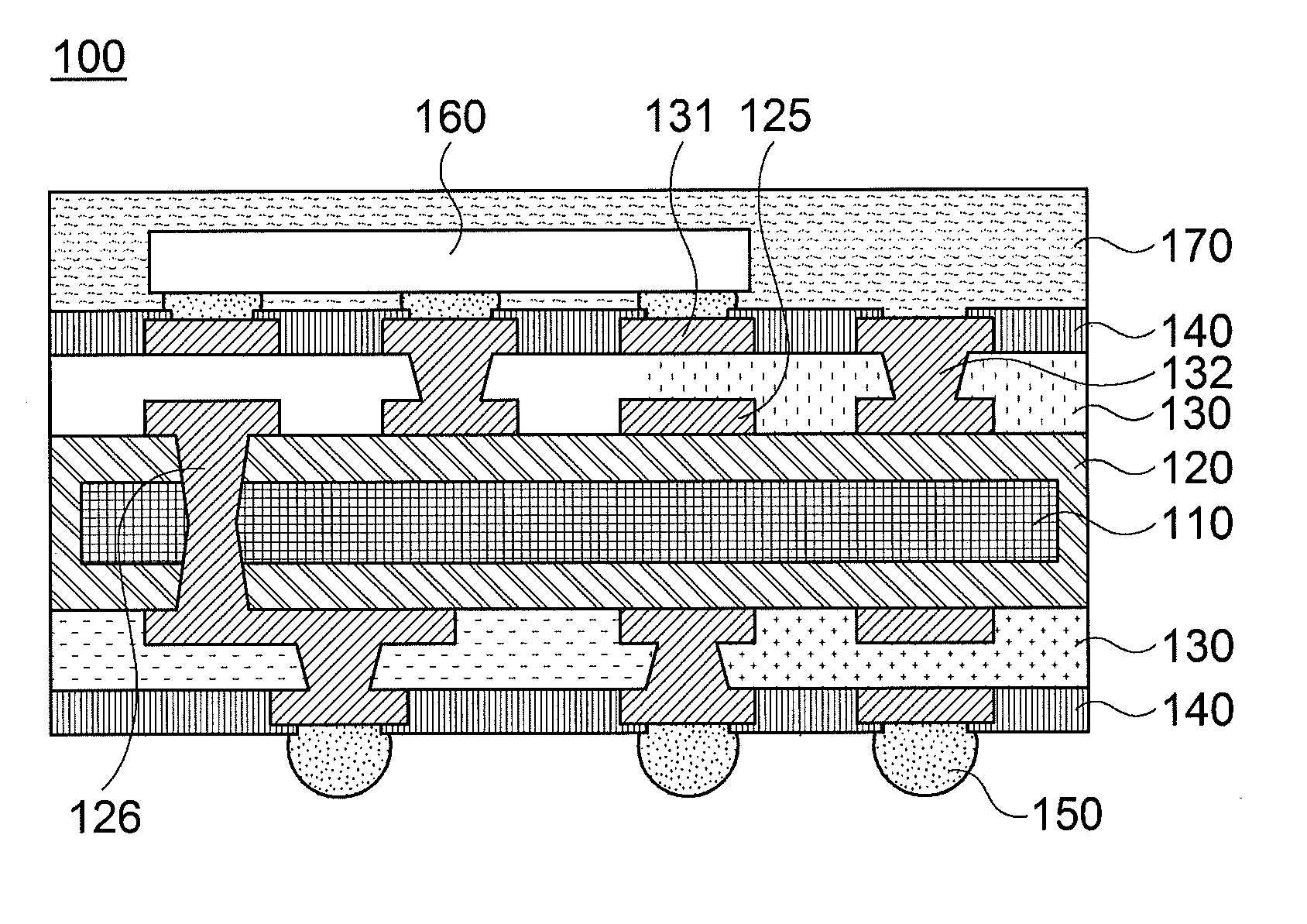
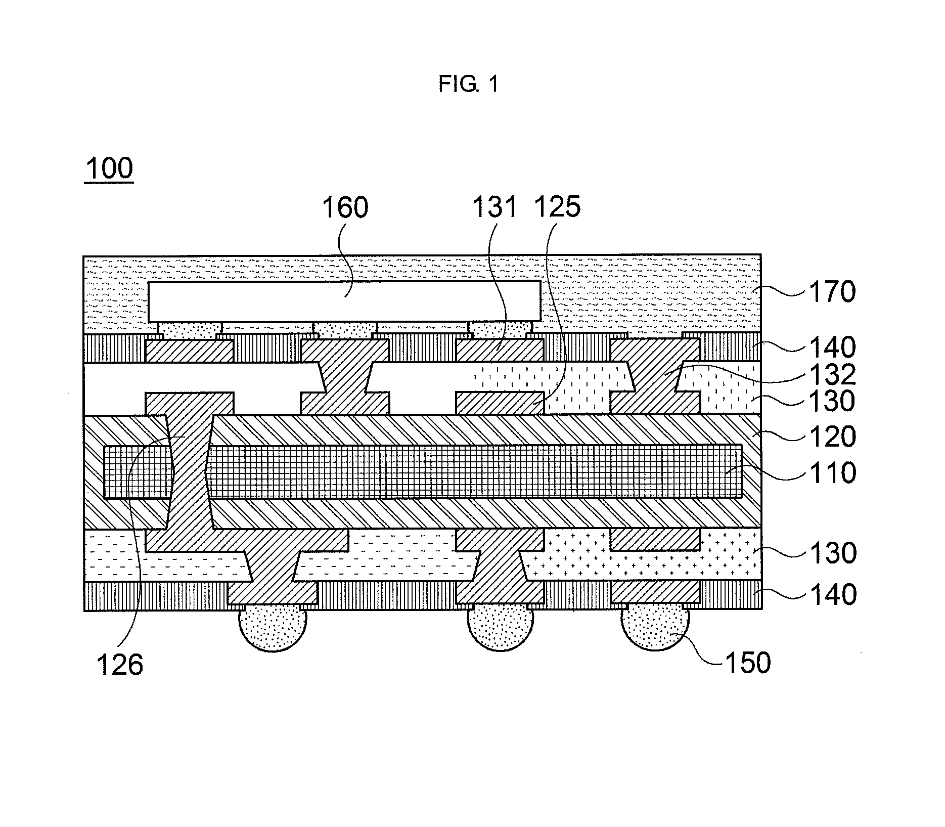
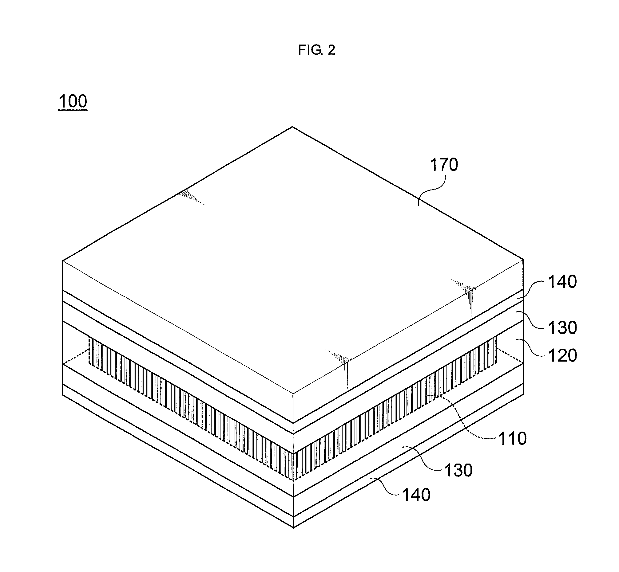
[0050]First, FIG. 1 is a cross-sectional view of a printed circuit board in accordance with an embodiment of the present invention, and FIG. 2 is a perspective view of the printed circuit board in accordance with an embodiment of the present invention.

[0051]As shown, a printed circuit board 100 according to the present invention may include a core 110 made of a glass material, an insulator 120 surrounding side surfaces and upper and lower surfaces of the core 110, an internal circuit layer 125 formed on the insulator 120, and a via 126 for connecting the internal circuit layers 125.

[0052]Further, a build-up layer 130 may be further formed on the insulator 120, and an e...


PUM


Abstract

A printed circuit board and a method of manufacturing the same. In one embodiment, a printed circuit board includes: a core made of a glass material; an insulator surrounding the core; and a via connecting internal circuit layers through the core and the insulator.

Description

CROSS-REFERENCE TO RELATED APPLICATIONS[0001]This application claims the foreign priority benefit under 35 U.S.C. Section 119 of Korean Patent Application Serial No. 10-2013-0136274, entitled filed Nov. 11, 2013, which is hereby incorporated by reference in its entirety into this application.BACKGROUND[0002]1. Field[0003]Embodiments of the present invention relate to a printed circuit board and a method of manufacturing the same, and more particularly, to a printed circuit board, which can prevent exposure of a side surface of a core, and a method of manufacturing the same.[0004]2. Description of Related Art[0005]In recent times, as the thickness of portable devices is being gradually decreased, there have been efforts to reduce the entire thickness of internal components by manufacturing a thin substrate on which a plurality of electronic components are mounted with the thinning of the electronic components mounted inside the portable devices.[0006]In particular, when manufacturing...

Claims


Application Information

Patent Timeline
Patent Type & Authority Applications(United States)
IPC IPC(8): H05K1/02H05K3/42H05K3/00H05K3/46H05K1/11H05K1/03
CPCH05K1/0271H05K2203/1327H05K1/115H05K1/0306H05K1/038H05K3/0067H05K3/0017H05K3/0044H05K3/4652H05K3/0014H05K3/429H05K2201/068H05K2201/026H05K2203/0235H05K2203/0323H05K2203/0703H05K2203/061H05K1/0298H05K3/0052H05K3/4605H05K2201/0195H05K3/002H05K3/0029H05K3/0047H05K3/007H05K3/4644H05K2201/017H05K2201/0187H05K2201/0909H05K2201/09136H05K2201/09827H05K2201/09881H05K2201/2009H05K2203/1536H01L24/97H01L2224/16225H01L2224/97H01L2924/15311H01L2924/12042H01L2224/81H01L2924/00H05K3/40H05K3/46
Inventor CHO, SUK HYEONNAM, HYO SEUNGLEE, YONG SAMAHN, SEOK HWAN
Owner SAMSUNG ELECTRO MECHANICS CO LTD
Why Eureka
Try Eureka