Prober

a technology of prober and stage member, applied in the field of prober, can solve the problems of energy efficiency deterioration, likely to occur, and deterioration of the measurement accuracy and achieve the effect of improving the measurement accuracy and reliability of the wafer level inspection and downsizing the stage member

Active Publication Date: 2015-05-21
TOKYO SEIMITSU
View PDF2 Cites 19 Cited by
  • Summary
  • Abstract
  • Description
  • Claims
  • Application Information

AI Technical Summary

Benefits of technology

[0021]Moreover, in a preferred mode of the present invention, the contactor is disposed as contactor groups formed with multiple contactors which are adjacent to each other, and the contactor groups are disposed at predetermined intervals. According to this mode, it becomes possible to downs

Problems solved by technology

However, in a case where the wafer chuck is heated or cooled for the heating or cooling of a chip, in the technique disclosed in Japanese Patent Application Laid-Open No. 2013-118320, since the wafer chuck has a structure in which a wafer holding portion and a probe contact area are integrated, not only the wafer holding portion but also the probe contract area is heated or cooled and therefore the energy efficiency deteriorates.
Moreover, the temperature change of

Method used


Image

  • Prober
  • Prober
  • Prober

Examples


example 1

Variation Example 1

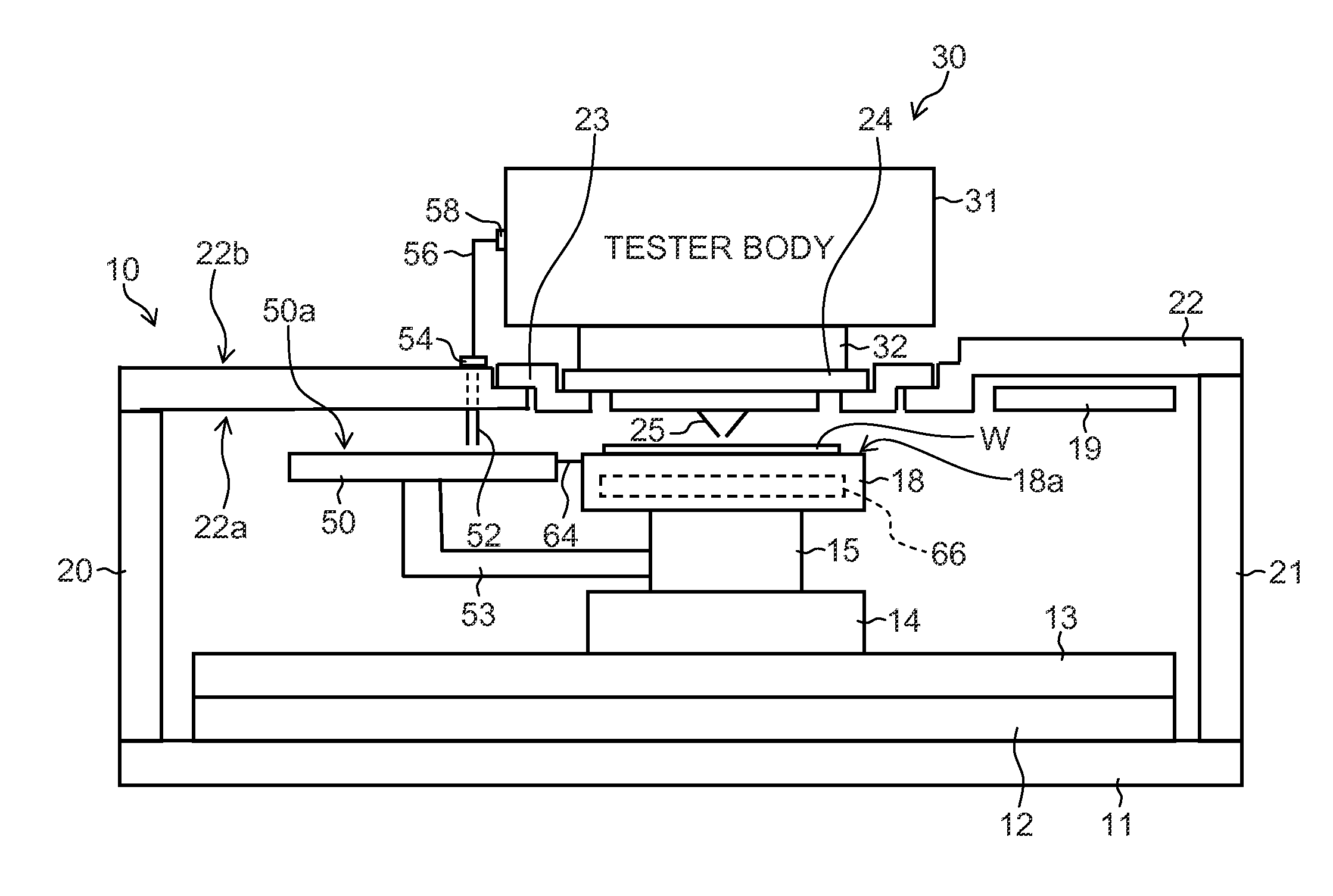
[0060]In the above-mentioned embodiment, the stage member 50 is configured so as to be fixed to a position adjacent to the wafer chuck 18, but the stage member 50 may be configured so as to be foldable.

[0061]For example, in the variation example illustrated in FIG. 4, the stage member 50 is configured so as to be rotatable around a rotation axis 70 installed in the edge part (edge part on the wafer chuck) of the stage member 50. That is, the stage member 50 is configured so as to be rotatable around the Y axis (the direction vertical to the surface of FIG. 4), and can transition between a state where the stage surface 50a is disposed to be parallel to the support surface 18a of the wafer chuck 18 (shown by the dotted line in FIG. 4) and a state where it is disposed to be vertical to it (shown by the solid line in FIG. 4).

[0062]According to a mode in which the stage member 50 is configured so as to be foldable in this way, at the time of load or unload and alignmen...

example 2

Variation Example 2

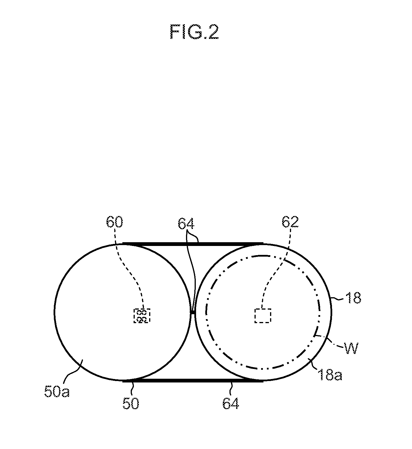
[0063]In the above-mentioned embodiment, as illustrated in FIG. 2, the stage surface 50a of the stage member 50 has the same shape and area as the support surface 18a of the wafer chuck 18, but the stage surface 50a may have a different shape or an area as long as the spring pins 52 can always come into contact with the stage surface 50a in at least a movable range of the wafer chuck 18. For example, a mode is possible in which the stage surface 50a of the stage member 50 has the same planar shape (circular shape) as the support surface 18a of the wafer chuck 18 and has a larger area than the support surface 18a. Moreover, as illustrated in FIG. 5, a mode is possible where the side surface of the stage member 50 on the side of the wafer chuck 18 is formed in a concave shape along the side surface of the wafer chuck 18. In any modes, the spring pins 52 always come into contact with the stage surface 50a in at least a movable range of the wafer chuck 18, and it is p...

example 3

Variation Example 3

[0064]In the above-mentioned embodiment, a configuration is shown in which the spring pins 52 are installed in the head stage 22 forming the chassis of the prober 10, but the spring pins 52 may be installed in a member held in the head stage 22, and, for example, as illustrated in FIG. 6, it is possible to adopt a configuration in which the spring pins 52 are installed in the probe card 24. In this case, the spring pins 52 are electrically connected with the tester body 31 through the contact ring 32. By this means, since the relative positional relationship between the spring pins 52 and the probe 25 does not change even if the wafer chuck 18 moves, it is possible to acquire an effect similar to the above-mentioned embodiment.


PUM


Abstract

A prober includes: a wafer chuck having a conductive support surface; a movement rotation mechanism which moves and rotates the wafer chuck; a head stage which holds a probe holding portion; a stage member which has a conductive stage surface that is formed in parallel to the support surface and electrically connected with the support surface, and can move integrally with the wafer chuck; and a contactor which is fixed to a position facing the stage member and whose tip can electrically come into contact with the stage surface, wherein the stage member is separated from the wafer chuck as a separate body, and the stage surface and the support surface are electrically connected through a wiring member; and a back-surface electrode of a chip is electrically connected with a tester through the wafer chuck, a wiring, the stage member and the contactor.

Description

BACKGROUND OF THE INVENTION[0001]1. Field of the Invention[0002]The present invention relates to a prober that performs an electrical inspection of multiple chips formed on a semiconductor wafer.[0003]2. Description of the Related Art[0004]In a semiconductor manufacturing process, various kinds of processing are applied to a thin disc-like semiconductor wafer, and multiple chips (dies) each having a semiconductor apparatus (device) are formed. The electrical characteristic of each chip is inspected, and then, after each chip is subsequently separated by a dicer, it is fixed to a lead frame or the like and assembled. The above-mentioned electrical characteristic inspection is performed by a wafer test system composed of a prober and a tester. The prober fixes a wafer to a wafer chuck and a probe is brought into contact with an electrode of each chip. For electrical inspection, the tester is electrically connected with the probe, applies current and voltage to each chip and measures t...

Claims


Application Information

Patent Timeline
IPC IPC(8): G01R1/04G01R31/26G01R31/28H01L21/683
CPCG01R1/0491H01L21/6831G01R31/2874G01R31/2601H01L21/6833G01R1/067G01R1/06777G01R31/2608
Inventor MURAKAMI, KONOSUKEMORI, TOSHIROSHIGESAWA, YUJIAOKI, KAZUHISAYAMAGUCHI, AKIRA
Owner TOKYO SEIMITSU
Why Eureka
Try Eureka