Solder joint material and method of manufacturing the same
a technology of joint material and manufacturing method, which is applied in the direction of manufacturing tools, solventing apparatus, transportation and packaging, etc., can solve problems such as bondability degradation
- Summary
- Abstract
- Description
- Claims
- Application Information
AI Technical Summary
Benefits of technology
Problems solved by technology
Method used
Image
Examples
first and second embodiments
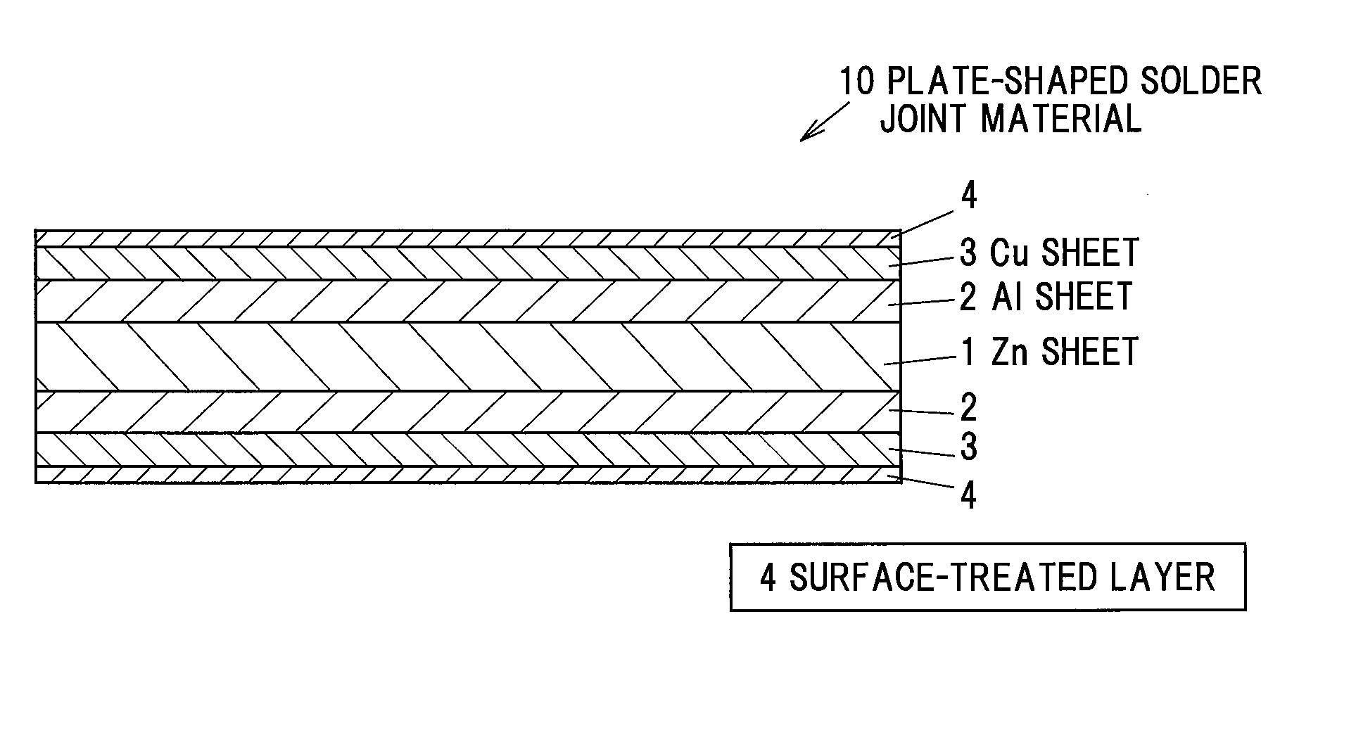
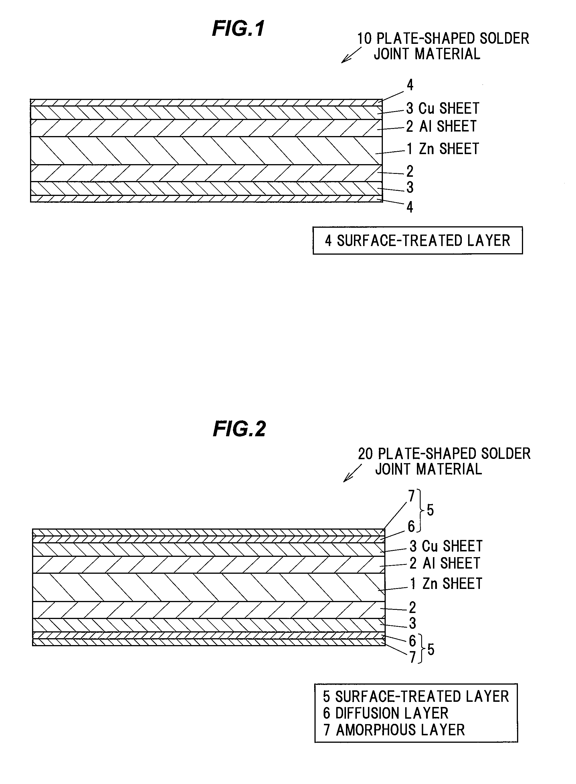
[0039]Solder joint materials in the first and second embodiments of the invention have a plate-like shape in which the Al-based metal material, the Cu-based metal material and the surface-treated layer are sequentially provided on each of a pair of opposing sides of the Zn-based metal material which has a rectangular cross section. The materials and layer here are provided on both sides of the Zn-based metal material but it is not limited thereto. The Al-based metal material, the Cu-based metal material and the surface-treated layer may be sequentially provided on only one side of the Zn-based metal material.
[0040]FIG. 1 is a schematic cross sectional view showing a solder joint material in the first embodiment of the invention and FIG. 2 is a schematic cross sectional view showing a solder joint material in the second embodiment of the invention.
[0041]A plate-shaped solder joint material 10 shown in FIG. 1 has the same configuration as that shown in FIG. 4 of JP-A 2012-71347 mentio...
third and fourth embodiments
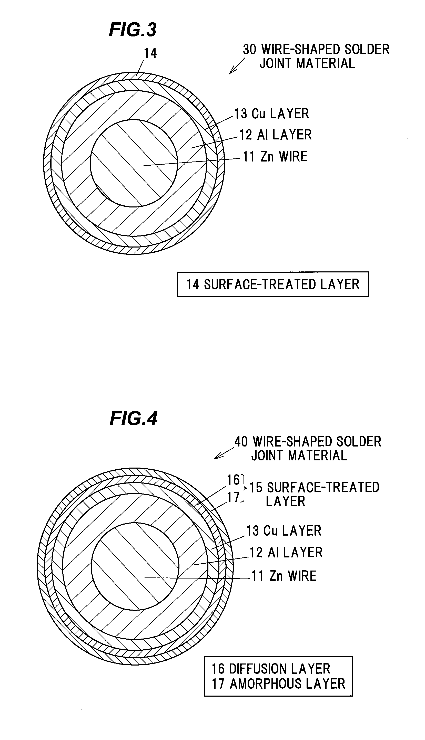
[0062]Solder joint materials in the third and fourth embodiments of the invention have a wire-like shape in which the Al-based metal layer covers an outer periphery of the Zn-based metal wire having a circular cross section, the Cu-based metal layer covers an outer periphery of the Al-based metal layer and the surface-treated layer covers an outer periphery of the Cu-based metal layer.
[0063]FIG. 3 is a schematic cross sectional view showing a solder joint material in the third embodiment of the invention and FIG. 4 is a schematic cross sectional view showing a solder joint material in the fourth embodiment of the invention.
[0064]A wire-shaped solder joint material 30 shown in FIG. 3 is provided with a Zn-based metal wire 11 (hereinafter, sometimes simply referred as “Zn wire”), an Al-based metal layer 12 (hereinafter, sometimes simply referred as “Al layer”) covering the outer periphery of the Zn wire 11, a Cu-base metal layer 13 (hereinafter, sometimes simply referred as “Cu layer”...
example 1
[0086]A 0.5 mm-thick flat sheet formed of pure copper (tough pitch copper; hereinafter, described as “TPC”) was prepared, a 0.002 μm-thick cover layer formed of zinc was then formed on a surface of the flat sheet by electrolytic plating and heat treatment was subsequently performed in the ambient air at a temperature of 50° C. for 10 minutes, thereby obtaining a sample provided with a surface-treated layer. Based on Auger analysis performed on the obtained sample from the surface in a depth direction, it was confirmed that a 0.003 μm-thick surface-treated layer composed of zinc (Zn), oxygen (O) and copper (Cu) was formed.
PUM
| Property | Measurement | Unit |
|---|---|---|
| thickness | aaaaa | aaaaa |
| thickness | aaaaa | aaaaa |
| temperature | aaaaa | aaaaa |
Abstract
Description
Claims
Application Information


