Optical film, manufacturing method thereof, and display device including the same

Active Publication Date: 2015-06-04
SAMSUNG ELECTRONICS CO LTD +1
View PDF7 Cites 4 Cited by
  • Summary
  • Abstract
  • Description
  • Claims
  • Application Information

AI Technical Summary

Benefits of technology

The patent text describes a compensation film that works well for certain wavelengths of light, but may not work well for other wavelengths. The patent aims to develop an optical film that reduces wavelength dependency and improves properties.

Problems solved by technology

In the case of the light emitting display device, for example, an organic light emitting diode (“OLED”), visibility and the contrast ratio may be deteriorated since the exterior light is reflected by a metal such as an electrode.
Since a compensation film is strongly dependent upon a wavelength of the incident light, it may operate well for light having a certain wavelength, but the effect may be deteriorated for other wavelengths of the incident light.

Method used


Image

  • Optical film, manufacturing method thereof, and display device including the same
  • Optical film, manufacturing method thereof, and display device including the same
  • Optical film, manufacturing method thereof, and display device including the same

Examples


example 1

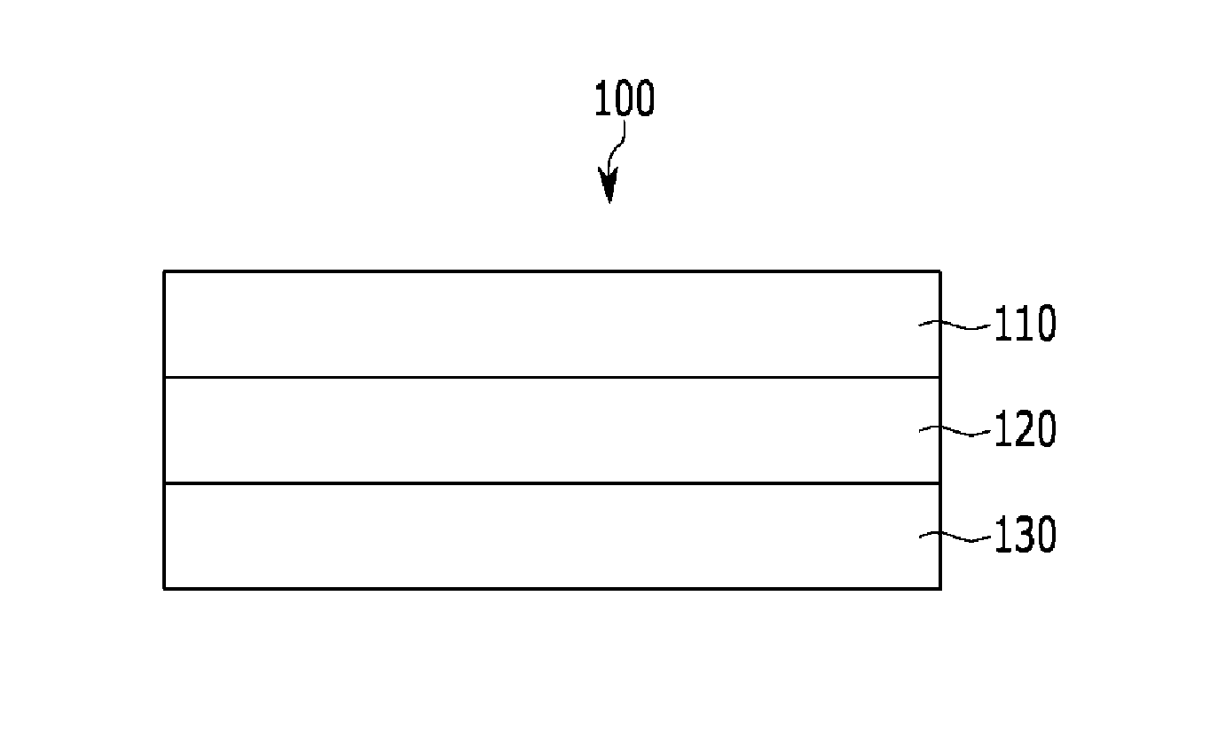
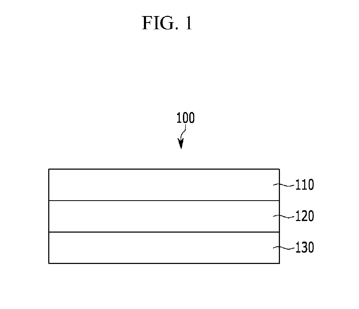
[0087](1) Preparation of Polarization Layer

[0088]A polyvinyl alcohol (“PVA”) film (PS 60, Kuraray) is stretched until it has a thickness of around 22 micrometers (μm), and a hard coating film (“DNP”) having a thickness of 40 μm is attached to one side of the stretched PVA film. The hard coating film has a shape in which hollow silica particles are coated on a TAC film.

[0089](2) Preparation of First Phase Delay Layer

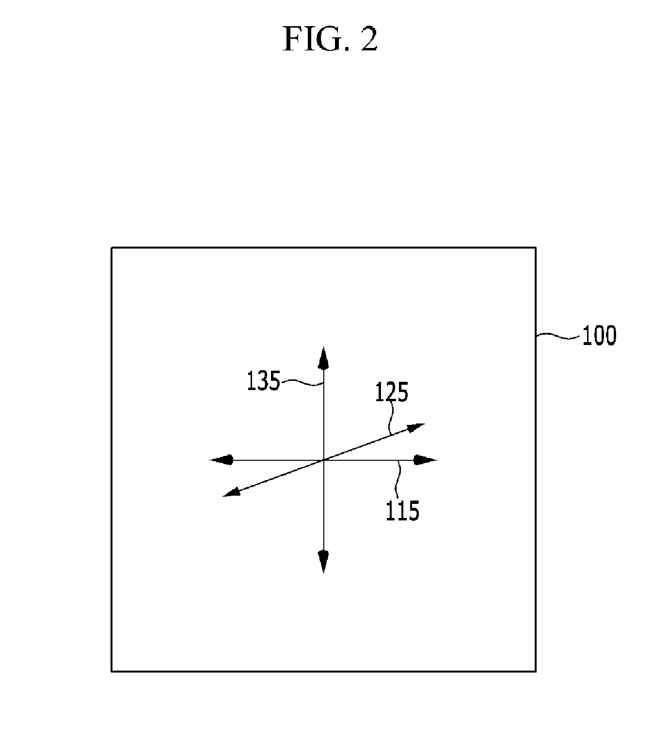
[0090]An alignment layer (polyacryl) is disposed on a triacetyl cellulose (“TAC”) film (Fuji Film) and rubbed in a 22.5 degree direction relative to the transmissive axis of the polarization layer. Subsequently, a liquid crystal solution including liquid crystal (RMM 1049, Merck) and toluene is coated on the rubbed alignment layer to a thickness of 3 μm. Subsequently, the coated liquid crystal solution is dried and irradiated with UV light to provide a first phase delay layer in which a liquid crystal layer is disposed on the TAC film.

[0091]The first phase delay layer is ...


PUM

PropertyMeasurementUnit
Thicknessaaaaaaaaaa
Thicknessaaaaaaaaaa
Angleaaaaaaaaaa

Abstract

An optical film including a polarization layer, a first phase delay layer positioned on a side of the polarization layer and including a liquid crystal, and a second phase delay layer positioned on a side of the first phase delay layer, where the first phase delay layer has an optical axis defining an angle of about 17 degrees to about 27 degrees or about −27 degrees to about −17 degrees relative to a transmissive axis of the polarization layer, and the second phase delay layer has an optical axis defining an angle of about 85 degrees to about 95 degrees relative to the transmissive axis of the polarization layer.

Description

CROSS-REFERENCE TO RELATED APPLICATION[0001]This application claims priority to Korean Patent Application No. 10-2013-0148543 filed on Dec. 2, 2013, and all the benefits accruing therefrom under 35 U.S.C. §119, the entire contents of which are incorporated herein by reference.BACKGROUND[0002]1. Field[0003]An optical film, a manufacturing method thereof, and a display device including the same are disclosed.[0004]2. Description of the Related Art[0005]Commonly used flat panel display may be classified into a light emitting display device emitting light by itself and a non-emissive display device requiring a separated light source, and an optical film such as a retardation film is frequently employed for improving an image quality thereof.[0006]In the case of the light emitting display device, for example, an organic light emitting diode (“OLED”), visibility and the contrast ratio may be deteriorated since the exterior light is reflected by a metal such as an electrode. In order to ef...

Claims


Application Information

Patent Timeline
IPC IPC(8): G02B5/30B32B38/00G02F1/13363B32B37/24B32B37/20G02F1/1335
CPCG02B5/3016G02B5/3083B32B37/20G02B5/305G02F1/133528G02F1/13363B32B2551/00B32B38/0012B32B2037/243B32B2307/42B32B2309/16B32B2038/0028B32B2457/202B32B37/24B32B37/203B32B2307/40
Inventor KIM, HYUNG JUNOH, KYOUNG AHLEE, MOON YEONJUNG, MYUNG SUP
Owner SAMSUNG ELECTRONICS CO LTD
Why Eureka
Try Eureka